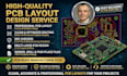
I will design pcb layout with schematic, footprints, gerber files and bom

United Kingdom

I speak English

Precision PCB Design for Reliable Electronics

Hello! I’m a professional PCB designer specializing in high quality schematic design and PCB layout for reliable, manufacturing ready electronics. I help startups, engineers, and businesses turn idea...
About this Gig

Looking for a reliable engineer to turn your circuit concept into a high performance, manufacturing ready PCB?

I provide end to end PCB design services using industry-standard tools (Altium, KiCad, EasyEDA) with a strong focus on Signal Integrity, Design for Manufacturing (DFM), and zero DRC errors.


What You Will Get:

  • Schematic Capture: Clean, structured circuit diagrams.
  • PCB Layout: Optimized trace routing, clearance, and noise reduction.
  • Custom Footprints: Accurate land patterns built to exact component datasheets.
  • Production Files: Gerber, Drill, and Pick & Place files (JLCPCB, PCBWay ready).
  • Bill of Materials (BOM): Sourcing ready component list with MPNs.
  • 3D Models: STEP files for enclosure design and fitting.


Why Choose Me?

  • 100% DFM & DRC Compliant: Zero production errors or costly board spins.
  • Industry Standard Quality: Tailored for fast turn fabrication.
  • Fast & Transparent Communication: Regular updates from start to finish.


Please contact me before placing an order to discuss your project requirements, scope, and custom pricing!

Specialization:

Circuit design

•

Schematics

•

Layout

•

Footprint

File format:

Gerber

•

SCH

•

3DS

Software:

Allegro

•

Altium Designer

•

Eagle CAD

•

EasyEDA

•

KiCad

Interface:

HDMI

•

I2S

•

SPI

•

I2C

•

Ethernet