Browse categories
Explore
Fiverr Pro
English
$
USD
ELECTRONICS AND ELECTRICAL ENGINEERING
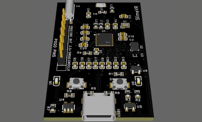
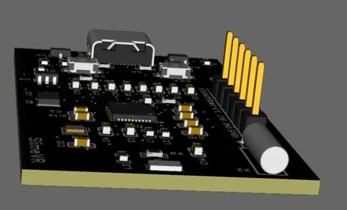
I'm an experienced PCB deslgn engineer focus in PCB layout, schematic design, PCB routing, circuit deslgn, Gerber files, and BOM generation for manufacturing. I deslgn single layer, multilayer, ESP32, IoT, embedded systems, high speed PCBs using KiCad, Altium Deslgner, and EasyEDA, delivering optimized, production ready designs with reliability, performance, manufacturability in mind.
Whether you need a new PCB from scratch or want to improve an existing deslgn, I can help transform your idea into a fully functional and manufacturing ready product.
What I Offer:
Why Choose Me?
Contact me before placing an order so we can discuss your project requirements and ensure the best solution for your deslgn!


Specialization:
Circuit design
•
Schematics
•
Layout
•
Footprint
•
Gerber
File format:
Gerber
•
BRD
•
SCH
•
3DS
•
Software:
Altium Designer
•
EasyEDA
•
KiCad
•
Proteus
What files do you need to start the PCB design?
I can work from schematics, hand drawings, requirements documents, block diagrams, or existing PCB files.
Which PCB design software do you use?
I primarily use KiCad, Altium Designer, and EasyEDA depending on project requirements.
Will I receive manufacturing ready files?
Yes. You will receive Gerber files, BOM, pick and place files, source files, and production documentation.
Can you design multilayer and high speed PCBs?
Yes. I design multilayer, RF, impedance controlled, and high-speed PCBs with proper routing practices.
Do you work on ESP32, Arduino, STM32, and IoT projects?
Yes. I design PCBs for ESP32, Arduino, STM32, sensors, wireless modules, and embedded systems.
Can you review and improve an existing PCB design?
Yes. I can review schematics and layouts, identify issues, optimize routing, and improve manufacturability