Browse categories
English
$
USD
Connect to your AI
PCB Design Engineer, Schematic Design, PCB Layout and High Quality Routing
Need a professional PCB layout from your electronic circuit schematic?
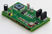
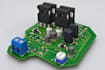
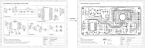
I will convert your circuit schematic into a well-organized PCB layout tailored to your project requirements. I focus on accurate component placement, clean routing, proper board arrangement, and design rule checks DRC to help identify layout issues before fabrication.
MY PCB SERVICES INCLUDE:
WHAT YOU WILL RECEIVE:
A professionally arranged PCB layout with the project files and manufacturing documents included in your selected package.
I pay close attention to your component list, board size, layer count, connection requirements, and output format to deliver a layout that meets your specifications.
Please contact me before ordering and share your schematic and project requirements so we can confirm the scope and right package.
Lets turn your circuit schematic into a professional PCB layout!
What do you need from me to get started?
I will need your electronic circuit schematic, component list (if available), board dimensions, layer requirements, and any specific project instructions.
Can you convert an existing circuit schematic into a PCB layout?
Yes! I can convert your existing electronic circuit schematic into a professional PCB layout with proper component placement, organized connections, and clean routing.
Do you provide manufacturing ready PCB files?
Yes. I can provide Gerber files, drill files, BOM, and other relevant manufacturing documents depending on your selected package.
Can you design single layer and multilayer PCBs?
Yes! I can work on single layer, double layer, and multilayer PCB layouts based on your project complexity and requirements.
Which PCB design software do you use?
I can work with professional PCB design tools such as Altium Designer, KiCad, EasyEDA, and Autodesk Fusion Electronics, depending on project requirements.
Will I receive the editable source files?
Yes. Editable project source files are included according to the package you select, allowing you to review and make future modifications.
Do you provide physical PCB manufacturing or prototyping?
My service focuses on schematic conversion, PCB layout, and preparation of manufacturing files. Physical fabrication and prototyping are not included unless separately agreed.


