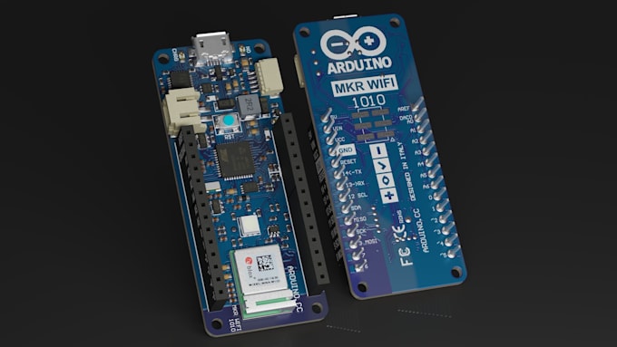
I will design pcb layout, schematics, multilayer pcb, kicad, esp32 and iot

Poland

I speak English, French

A dedicated Electronics Engineer and PCB Designer

I am a dedicated Electronics Engineer & PCB Designer with 8 years of experience and a relentless drive to stay ahead of every industry advancement. Specialized in schematic capture, PCB layout, elect...
About this Gig

Are you looking for a professional PCB deslgn engineer who can turn your electronic idea into a fully functional and manufacturing ready circuit board? You are in the right place.


I will deslgn high quality PCB layouts, schematic circuits, and production ready files using KiCad and other professional tools. I specialize in creating accurate, efficient, and industry standard deslgns suitable for prototypes and mass production.

Services

  • Schematic capture
  • 2-layer & multilayer board design
  • KiCad projects
  • ESP32, Arduino & STM32 hardware
  • IoT device development
  • Circuit redesign and optimization
  • DRC verification
  • Gerber, BOM & Pick-and-Place files


You'll Receive

  • Complete schematic
  • Optimized layout
  • KiCad source files
  • Gerber package
  • BOM
  • Pick-and-Place files (if needed)
  • Technical support

Whether you need a simple circuit or a complex PCB deslgn, I am ready to help you build it professionally.


Lets turn your idea into reality. Message me now so we can discuss your project requirements Thanks.

Specialization:

Circuit design

•

Schematics

•

Layout

•

Footprint

File format:

Gerber

•

STEP

•

VRML

•

BRD

•

SCH

Software:

Altium Designer

•

Eagle CAD

•

EasyEDA

•

KiCad

•

AutoCAD

Interface:

HDMI

•

MIPI DSI/CSI

•

I2S

•

TDM

•

UART

•

SPI

•

I2C

•

Wi-Fi

•

BLE

•

BT

•

GSM/GPRS