Browse categories
English
$
USD
Connect to your AI
rf pcb engineering, antenna design, firmware embedded and prototype development
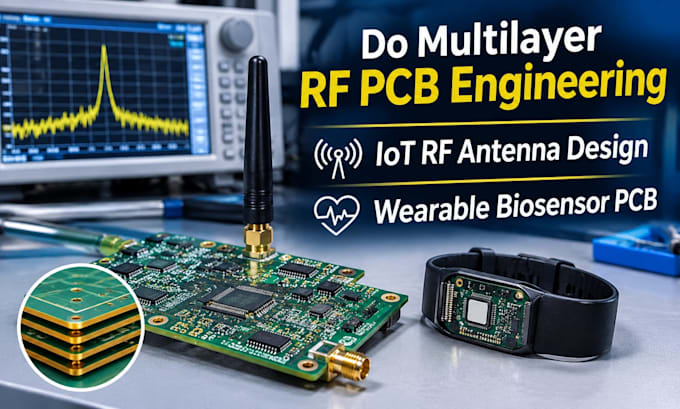
I specialize in multilayer RF PCB engineering, IoT antenna design, and wearable biosensor electronics, helping transform complex ideas into practical, efficient, and manufacturable hardware solutions.
From initial schematics and circuit development to PCB layout, RF simulation, antenna optimization, and prototype support, I provide engineering solutions to your technical requirements.
MY SERVICES INCLUDE:
SOFTWARES
DELIVERABLES
Send me a message before ordering!
1. What types of RF PCB designs do you offer?
I offer 2-layer, 4-layer, 6-layer, and advanced multilayer RF PCB designs for IoT devices, wireless communication systems, RF hardware, and custom electronics applications.
2. Can you design custom RF antennas for IoT devices?
Yes! I design and integrate custom RF antennas for IoT applications, including antenna tuning, impedance matching, simulation, and performance optimization.
3. Do you design wearable biosensor PCBs?
Yes. I develop wearable biosensor PCB solutions, including sensor interfaces, signal conditioning circuits, low-power electronics, and wireless connectivity integration.
4. Which software do you use for RF PCB design and simulation?
I use Altium Designer, KiCad, Cadence Allegro, CST Studio Suite, Ansys HFSS, Keysight ADS, and MATLAB, depending on project requirements.
5. What deliverables will I receive after project completion?
You can receive complete schematics, PCB layout files, Gerber files, BOM, antenna simulation results, design reports, and prototype support, depending on your selected package.
