Browse categories
Explore
Fiverr Pro
English
$
USD
Professional PCB and Embedded Systems Engineer, Altium Designer, KiCa and STM32
Do you have an existing PCB that needs to be recreated, modified, repaired, or converted into an editable design?
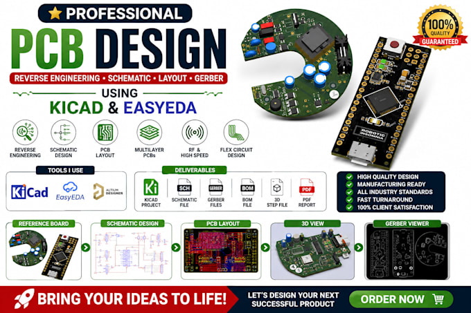
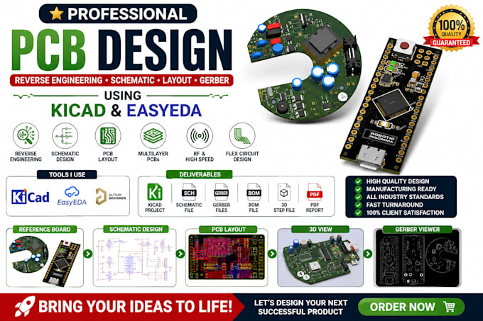
I'm Galusson, a PCB design specialist with 5+ years of experience in PCB reverse engineering, schematic reconstruction, PCB layout, and manufacturing-ready documentation. I can work from physical PCB boards, images, scans, existing Gerber files, or available files.
My service includes tracing connections, identifying components, recreating the schematic, rebuilding the PCB layout, assigning footprints, routing the board, and preparing fabrication-ready outputs. I focus on accurate connectivity, component placement, routing quality, and design-rule requirements.
What you can receive:
I use KiCad and EasyEDA to create organized, editable, and production-ready designs.
Whether you need to reproduce an obsolete board, recover an existing design, prepare a replacement PCB, or modify your current hardware, I'm ready to help.
MESSAGE ME TODAY FOR YOUR PROJECT!!!



Can you reverse engineer a PCB from photos or physical boards?
Yes. I can recreate the PCB layout and schematic from clear PCB photos, physical board information, measurements, or other available references
Can you convert Gerber files into editable PCB files?
Yes. I can use available Gerber files to recreate an editable PCB layout and prepare the required design files in KiCad or EasyEDA
Can you recreate the schematic and PCB layout?
Yes. I can reverse engineer both the schematic and PCB layout while matching components, connections, footprints, traces, and board dimensions as closely as the available information allows.
What software do you use?
I primarily use KiCad and EasyEDA for PCB reverse engineering, schematic capture, PCB layout, and manufacturing-ready file preparation.