Browse categories
Explore
Fiverr Pro
English
$
USD
WELCOME TO MY GIG
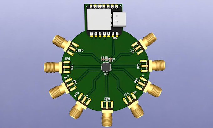
I will design RF antenna PCBs with a focus on antenna integration, impedance matching, RF routing and clean high-frequency layout.
This service is suitable for WiFi, Bluetooth, LoRa, GSM, GPS/GNSS and other RF applications where antenna performance and board layout matter. I can integrate it into your board and organize the RF path around your requirements. Send your target frequency, antenna type, board size, stackup and reference files.
WHAT I OFFER:
I use Altium Designer, KiCad and Cadence/OrCAD, delivering editable source files, schematic, PCB layout, BOM, Gerbers, drill files and fabrication-ready outputs.
Let's create a clean RF antenna PCB ready for engineering review and production. I keep the antenna feed, matching section and documentation organized, helping your team review the RF path, prototypes and refine the design efficiently. This keeps communication clear from design review through prototype and manufacturing!!!!
Can you design a PCB antenna?
Yes. I can work with PCB, microstrip and other antenna approaches based on the frequency and application.
Can you design impedance matching?
Yes. Matching networks can be included when the antenna, frequency and required performance information are available.
Do you support WiFi and Bluetooth antennas?
Yes. I can work on antenna integration for WiFi, Bluetooth, LoRa and other wireless applications.
Can you integrate an existing antenna?
Yes. Send the antenna specification, reference design or manufacturer recommendations.
Can you provide editable files?
Yes. Editable PCB/source files can be provided according to the selected package.
