Browse categories
Explore
Fiverr Pro
English
$
USD
Electrical Engineering Consultant
Struggling with EMI, signal loss, or crosstalk ruining your RF prototype?
Poor high-speed PCB layout kills range, bandwidth, and certification. I fix that.
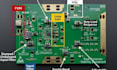
I am a Top-Rated Electronic Engineer specializing in High-Speed and RF PCB Design (Altium and KiCAD). I deliver manufacturing-ready layouts that pass EMC the first time.
What I deliver :
Software I use:
Your final deliverables (all tiers):
Message me BEFORE ordering.

Can you handle NDAs and keep my RF design confidential?
Yes. I sign NDAs gladly (yours or mine). I work on a locked, offline workstation. No cloud storage unless you approve. Source files are deleted 14 days after final delivery unless you request archiving
Do you run simulations for signal integrity before fabricating?
Absolutely. For Standard and Premium tiers, I perform pre-layout impedance calculations (Si9000e) and post-layout TDR simulations. For RF designs, I verify return loss and crosstalk. Eye diagram analysis is included for Premium.
Is your design ready for manufacturing (DFM/DFA)?
Yes. All Gerbers and stackups follow IPC-2221 and IPC-6012 Class 2/3 standards. I can tailor clearances, hole sizes, and annular rings to your specific fab house (JLCPCB, PCBWay, Eurocircuits, etc.). No unexpected fabrication holds.
What frequency range can you handle, and do you support mixed RF and digital?
I routinely design up to 6 GHz (RF) and 10 Gbps (digital). Mixed-signal boards (RF front-end plus FPGA plus power) are my specialty. I provide proper ground partitioning, stitching vias, and keep-out zones to prevent digital noise injection into RF paths.


