Browse categories
Explore
Fiverr Pro
English
$
USD
Need a professional PCB design that is clean, organized, and ready for manufacturing?
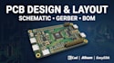
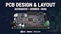
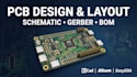
I will design a professional PCB layout, circuit schematic, and board de-sign based on your project requirements. Whether you are developing an IoT device, embedded system, prototype, controller, or custom electronics product, I can help turn your circuit idea into a structured PCB design.
What you can get:
I can work with popular PCB design workflows such as KiCad, Altium Designer, EasyEDA, and other suitable tools, depending on your project requirements.
Why work with me?
I focus on clean layouts, organized schematics, practical component placement, and clear project deliverables so your de-sign is easier to review and manufacture.
Whether you already have a schematic or need the PCB developed from your circuit requirements, choose the package that matches your project.
Send your project details and let's get started.
Can you convert my schematic into a PCB layout?
Yes. I can convert a suitable schematic into a properly organized PCB layout based on your specifications.
Which PCB software can you work with?
I can work with tools such as KiCad, Altium Designer and EasyEDA, depending on the requirements of the project.
Will I receive Gerber files?
Yes. Gerber files can be included in packages that specify manufacturing-ready files.
Can you design multilayer PCBs?
Yes. Multilayer PCB design can be included in the Standard or Premium package depending on the board complexity.
Can you work from an existing circuit or idea?
Yes. Please provide your schematic, circuit diagram, component information, reference design, or project requirements so the scope can be determined accurately.


