Browse categories
Explore
Fiverr Pro
English
$
USD
Senior RF and PCB Design Engineer, Custom Antennas and IoT Hardware
A compact wireless device can meet every PCB requirement and still suffer from poor range, unstable connectivity, or antenna detuning because of incorrect RF geometry, ground-plane interference, or impedance mismatch.
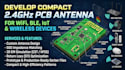
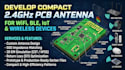
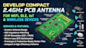
I develop compact 2.4GHz PCB antenna solutions for WiFi, BLE, IoT sensors, wearables, smart devices, and embedded wireless products. Each design considers available PCB space, antenna placement, ground clearance, feed-line routing, and matching-network integration to support reliable RF performance.
What I can design:
What I will provide: Custom antenna layout, RF routing guidance, matching-network details, and design files
Why choose me: Engineering-focused designs that address real RF layout and integration challenges
Message me before ordering
Thanks
1. What design software do you use for the PCB antenna layout?
I primarily work with Altium Designer, KiCad, and Autodesk Eagle. If you are using a different EDA software, please message me before ordering to confirm compatibility.
2. What files will I receive upon completion?
Depending on your package, you will receive production-ready Gerber files, PCB layout files, a layout guidance document detailing keep-out zones and ground clearance, and matching network component placement recommendations
3. Do you provide electromagnetic (EM) simulations for the antenna?
Yes! My Standard and Premium packages include simulation support and antenna tuning optimization to ensure a proper 50-ohm match and optimal radiation patterns before fabrication
4. What information do you need from me to get started?
To get started, I’ll need your schematic (or a block diagram), your board stack-up/layer count, available PCB real estate/dimensions, and any specific enclosure or casing constraints that might affect antenna performance