Browse categories
Explore
Fiverr Pro
English
$
USD
Turning Ideas Into Production Ready Electronics and Mechanical Products
Are you dealing with signal integrity, impedance, crosstalk, EMI, or high-speed routing issues in your PCB? I can help turn your design into a clean, reliable, and manufacturing-ready RF or high-speed PCB.
I'm an Electronics Engineer specializing in:
I can work with interfaces such as:
My services include:
I focus on practical layout decisions that help prevent costly PCB revisions and improve signal quality, manufacturability, and overall board reliability.
Send your:
Contact me before ordering, and I'll review your requirements and confirm the right approach.
Thank you!
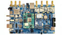
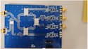

Can you design RF and high-speed PCB layouts?
Yes. I can design RF and high-speed PCB layouts with attention to controlled impedance, differential pairs, grounding, routing, clearances, and manufacturability.
Which high-speed interfaces can you work with?
I can work with interfaces such as USB/USB-C, HDMI, Ethernet, PCIe, MIPI, Wi-Fi, and other high-speed digital signals, depending on the project requirements.
Can you handle controlled impedance routing?
Yes. I can implement controlled-impedance routing based on your required impedance, stackup, dielectric properties, trace geometry, and PCB manufacturer's capabilities.
Can you design differential pairs?
Yes. I can route differential pairs with appropriate spacing, length matching where required, reference planes, and routing constraints based on the interface specifications.
Do you provide PCB stackup guidance?
Yes. I can help determine an appropriate layer structure and routing approach based on your signal requirements, impedance targets, board size, and manufacturing capabilities.
Can you work with RF antennas and RF signals?
Yes. I can handle RF routing, antenna connections, ground clearances, via stitching, and layout considerations based on the component or antenna manufacturer's requirements.
Can you fix an existing high-speed or RF PCB?
Yes. I can review an existing design and identify layout concerns related to routing, impedance, grounding, component placement, clearances, and manufacturability.
Which PCB design software do you use?
I work with Altium Designer, KiCad, and EasyEDA, depending on the project and required source-file format.
What do you need before starting an RF or high-speed PCB project?
Please provide the schematic, board dimensions, required interfaces, impedance targets, component datasheets, PCB manufacturer specifications, preferred stackup, and any existing design files or layout constraints.


