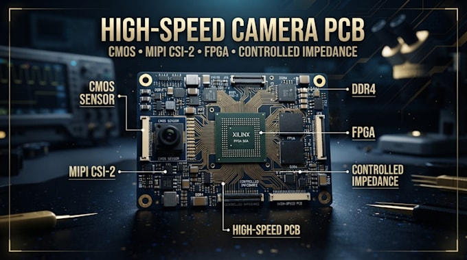
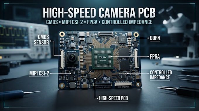
I will do high speed camera pcb with cmos sensor mipi csi fpga and controlled impedance

United Kingdom

I speak English

Professional PCB Design and Hardware Engineering Specialist

I’m a professional PCB Engineer specializing in advanced schematic capture, multilayer PCB layout, RF/wireless hardware, embedded systems, high-speed electronics, and manufacturing-ready Gerber files....
About this Gig

Welcome To My Gig Description


Develop a high-speed camera PCB engineered for advanced imaging, embedded vision, machine vision, and FPGA-based camera systems. I will create a reliable hardware solution integrating CMOS image sensors, MIPI CSI/CSI-2, FPGA interfaces, controlled impedance routing, high-speed differential pairs, and optimized power distribution.


I focus on signal integrity, component selection, PCB stackup, routing constraints, and manufacturability to produce a professional hardware platform suitable for prototyping and production.


What I Offer

  • CMOS image sensor integration
  • MIPI CSI/CSI-2 interface
  • FPGA integration
  • High-speed differential-pair routing
  • Controlled impedance routing
  • Multilayer PCB development
  • DDR/SDRAM interface support


Why Choose Me?

I approach every project with attention to high-speed signal integrity, impedance control, thermal considerations, component availability, and manufacturing requirements, ensuring the PCB is structured for reliable real-world implementation.


Ideal For
  • Industrial cameras
  • Machine vision systems
  • Embedded vision
  • AI camera hardware
  • FPGA camera platforms
  • Robotics vision
  • UAV/drone cameras
  • Inspection systems


Specialization:

Circuit design

•

Schematics

•

Layout

•

Footprint

File format:

Gerber

•

STEP

•

SCH

•

PDF

•

ODB

Software:

Altium Designer

•

Eagle CAD

•

EasyEDA

•

Fusion 360

•

KiCad

Interface:

HDMI

•

MIPI DSI/CSI

•

I2S

•

UART

•

SPI

•

I2C

•

PCIe

•

Wi-Fi

•

BLE

•

LTE