Browse categories
Explore
Fiverr Pro
English
$
USD
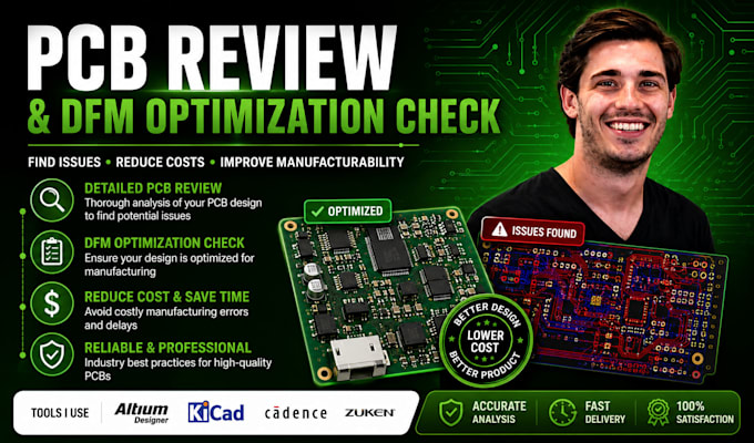
Manufacturing Ready PCB Design, High Speed Circuit Layouts
Are you about to send your PCB design to a manufacturing house like JLCPCB or PCBWay, but want to ensure there are zero costly mistakes? A single footprint error or trace clearance issue can ruin an entire production run.
I am a professional electronics engineer providing comprehensive PCB review and DFM optimization checks. I will rigorously audit your design files to catch manufacturing errors, trace issues, and component placement mistakes before you click order.
What I inspect during your professional PCB review:
- Complete Design Rule Checks (DRC) for clearance and trace width
- Component footprint validation against official manufacturer datasheets
- Design for Manufacturability (DFM) alignment for smooth factory assembly
- Signal integrity, ground planes, and thermal management optimization
- Solder mask and silkscreen legibility review
Don't risk wasting thousands of dollars on non-functional hardware prototypes. Let an expert engineer verify your Altium or KiCad projects first. You will receive a detailed PDF feedback report with annotated screenshots outlining necessary corrections.
Please message me with your project parameters before placing your order!

What file formats do I need to provide for the PCB review?
For the most thorough engineering audit, please provide your native design project files (Altium Designer, KiCad, or EasyEDA). If you cannot share the source design files, I can conduct the review using standard ODB++ directories or complete manufacturing Gerber files (including NC Drill files)
What exactly will I receive at the end of the PCB review?
You will receive a professional, comprehensive Engineering Audit Report in PDF format. This report includes annotated high-resolution screenshots of your layout highlighting exact error locations, a itemized checklist of Design Rule Check (DRC) and Design for Manufacturability (DFM) violations.
Will you directly modify my design files to fix the discovered errors?
The Basic and Standard tiers provide detailed feedback documentation so you can update your own files. However, the Premium tier includes direct file layout modifications. If you are on a lower tier and prefer that I implement the design fixes for you, I can easily send a custom add-on offer
Can you check high-speed digital interfaces or RF layout constraints?
Yes. Under the Premium tier, I conduct advanced reviews covering controlled impedance traces, differential pair phase matching, cross-talk mitigation, decoupling capacitor placement, and ground plane isolation for RF/EMI shielding.
Can you optimize my design for a specific manufacturing facility?
Absolutely. If you specify your preferred fabrication and assembly vendor (such as JLCPCB, PCBWay, or Advanced Circuits), I will audit your layout using that specific factory's precise minimum trace width, spacing, annular ring, and solder mask clearance tolerances to guarantee zero production delay
