Browse categories
Explore
Fiverr Pro
English
$
USD
PCB And Embedded Systems Engineer
Hello.
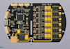
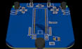
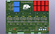
Is your PCB stuck at the schematic stage, difficult to route, missing correct footprints, or producing errors during design checks? Maybe you have an ESP32/STM32 idea, IoT prototype, or circuit that needs to become a clean, manufacturable PCB. I can help turn your concept or existing design into a professional PCB.
WHAT I OFFER
SOFTWARE
KiCad Altium Designer EasyEDA Autodesk Eagle. e.t.c
WHY CHOOSE ME?
I focus on organized schematics, accurate footprints, clean routing, design-rule checks and manufacturing-ready documentation, with clear communication throughout the project.
PERFECT FOR
IoT devices, ESP32/STM32 projects, Arduino electronics, sensors, robotics, automation, prototypes and custom electronic products.
Please send your schematic, circuit, requirements or reference files before ordering. I'll review the project and recommend the right PCB design package for your needs.
Kindly message me first.

What do you need to start my PCB project?
Please send your schematic, circuit diagram, requirements, reference PCB, datasheet, or any available project files. If you are starting from an idea, describe the required functions and I can advise on the design approach.
Can you design an ESP32 or STM32 PCB?
Yes. I can design custom PCB hardware around ESP32, STM32, Arduino, and other microcontrollers, including required footprints, power sections, connectors, sensors, and communication interfaces.
Can you create a PCB from my existing schematic?
Yes. I can convert your schematic into a professional PCB layout, including component placement, routing, footprint assignment, and design-rule checking.
Can you create custom footprints?
Yes. I can create or modify PCB footprints when a suitable library footprint is unavailable, based on the component datasheet and mechanical dimensions.
Do you provide Gerber and manufacturing files?
Yes, when included in your selected package. Depending on the project, deliverables can include Gerber, NC Drill, BOM, Pick & Place, schematic, PCB source files, and PDF documentation.
Which PCB design software do you use?
I primarily work with KiCad, Altium Designer, EasyEDA, and Autodesk Eagle, depending on the project requirements.
Can you design multilayer PCBs?
Yes. I can work on single-, double-, and multilayer PCB layouts. The required layer count and complexity will determine the appropriate package.
Can you redesign or modify an existing PCB?
Yes. I can modify existing PCB layouts, improve routing, replace components, update footprints, and prepare the design for manufacturing.
Can you design IoT and embedded PCBs?
Yes. I can design hardware for IoT and embedded applications involving ESP32, STM32, Arduino, sensors, communication modules, and other electronic components.
Should I contact you before placing an order?
es. Please contact me before ordering. PCB complexity varies significantly, so I can review your requirements and recommend the correct package and delivery time.


