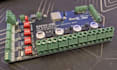
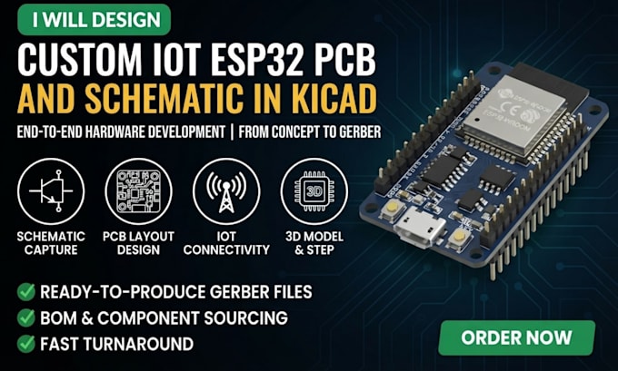
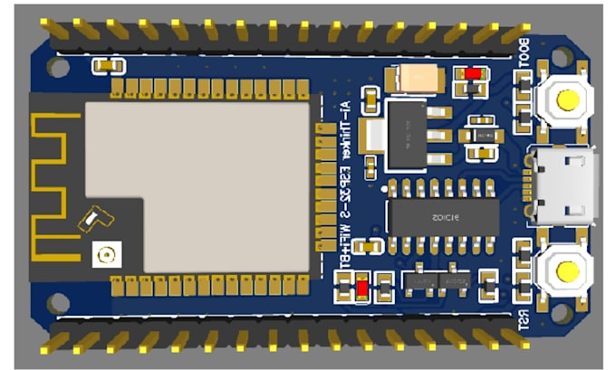
I will design custom iot esp32 pcb and schematic in kicad

United States

I speak English

Embedded firmware and software developer

I'm Henderson. I'm a Senior System Engineer with a solid background in embedded software and computer aided engineering. I spend my time working on hardware software integration, system design, and PC...
About this Gig

Building a custom IoT device or ESP32 prototype is stressful enough without your circuit board failing the moment you power it up. Dealing with unexpected signal noise, routing mistakes, or finding out your manufacturing files are broken after waiting a week for boards is a fast way to burn through your budget and timeline.


You need a clean, reliable layout that goes straight from your schematic to the factory floor without any headaches.


That is exactly what you get here. I will take your project specs and turn them into a professional, production ready board using KiCad, making sure everything is fully verified before a single trace gets etched.


Here is what will be delivered to your inbox:

  • A clean, well organized schematic and custom footprints built from scratch
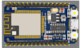
  • A precise multilayer PCB layout tuned specifically for ESP32 and wireless IoT performance
  • Complete Gerber files, drill files, a detailed BOM, and pick and place data ready for JLCPCB or PCBWay
  • Accurate 3D STEP models so you can check your enclosure fit before ordering


Send a message with your project details or schematic right now and let us get your board built right.
Specialization:

Circuit design

•

Schematics

•

Layout

•

Footprint

File format:

Gerber

•

STEP

•

SCH

•

3DS

•

PDF

Software:

Altium Designer

•

Eagle CAD

•

EasyEDA

•

KiCad

•

SolidWorks

Interface:

HDMI

•

MIPI DSI/CSI

•

I2S

•

TDM

•

UART

•

USB

•

SPI

•

I2C

•

SDIO

•

PCIe

•

Wi-Fi

•

BLE