Browse categories
Explore
Fiverr Pro
English
$
USD
Professional PCB Designer ,FPGA Embedded Systems Engineer
Level 1
Has met certain performance criteria and shows strong potential in the marketplace.
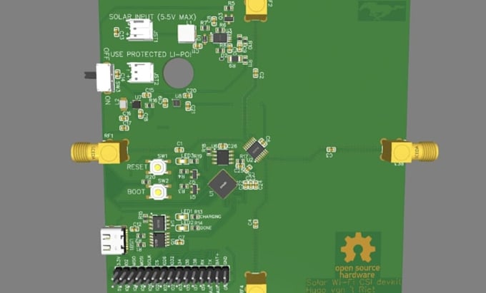
I design custom PCB solutions for electronics products, IoT devices, and wearables. Whether you need a new board designed from your schematic or a complete PCB layout developed around your circuit requirements, I can help turn your concept into a production ready design.
My service covers;
ESP32 PCB, RF PCB layout, wearable PCB, GPS PCB, IoT board, sensor interfaces, power management, communication circuits, and compact electronics.
I focus on component placement, routing, signal integrity, power distribution, grounding, thermal considerations, RF requirements, and design rule checks for very reliable and manufacturable boards.
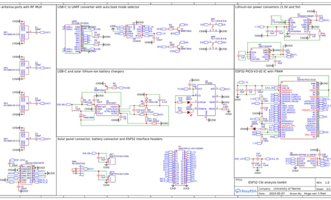
Depending on your project, I can provide schematic capture, PCB layout, component selection support, footprint creation, DRC checks, BOM, Gerber files, drill files, and manufacturing documentation.
I work with KiCad, Altium Designer, EasyEDA, and other common PCB design tools.
Send me your schematic, requirements, existing PCB files, or project idea, and I will review the details and help define the right approach for your board.
I can also improve existing layouts and prepare your design for manufacturing.

What information do you need to start the PCB design?
Please send your schematic, circuit requirements, component list, existing PCB files, dimensions, and any manufacturing requirements you have.
Can you design an ESP32 or GPS PCB from scratch?
Yes. I can develop the schematic and PCB layout based on your requirements, including component placement, routing, and design checks.
Can you work on RF and wearable PCB layouts?
Yes. I can design compact RF and wearable PCBs while considering routing, grounding, placement, signal integrity, and space limitations.
What files will I receive after the project is completed?
Depending on your package, you can receive source files, Gerbers, drill files, BOM, schematic, PCB layout, and manufacturing documentation.
Can you modify or fix an existing PCB design?
Yes. I can review your existing PCB, identify layout or DRC issues, make required modifications, and prepare it for manufacturing.