Browse categories
Explore
Fiverr Pro
English
$
USD
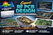
Professional PCB Designer ,FPGA Embedded Systems Engineer
Are you looking for expert rf pcb design and high-performance electronics development ? I deliver professional pcb design, pcb layout, and advanced rf pcb solutions for startups, IoT innovators, and hardware companies that demand precision and reliability.
With extensive experience in circuit deslgn, schematic design, antenna deslgn, and multilayer pcb development, I create production-ready boards optimized for signal integrity, impedance control, EMI/EMC compliance, and high-speed performance. Whether you need an esp32 pcb, STM32 system, IoT PCB deslgn, power electronics, or high frequency RF circuit, I provide complete hardware deslgn from concept to gerber files.
Tools include Altium Designer, KiCad, EasyEDA, OrCAD, ADS, HFSS, and CST for accurate RF simulation and thermal analysis. I also offer firmware development for embedded systems to ensure seamless hardware-software integration.
Youll receive clean schematics, optimized circuit layout, manufacturing-ready files, and professional support throughout prototyping and production.
If you need reliable, high-quality rf pcb design that meets 2026 industry standards, lets build your next innovation.

What information do you need before starting my RF PCB design project?
To begin any rf pcb design or multilayer PCB project, I require your project specifications, target frequency, board size constraints, power requirements, preferred MCU (ESP32/STM32/etc.), and application details. Clear requirements ensure accurate schematic design and prevent costly redesigns.
Do you provide both hardware and firmware development?
Yes. I offer complete hardware design and firmware development for embedded systems. This includes schematic design, PCB layout, and firmware integration to ensure seamless hardware–software performance.
Can you design high-speed or multilayer PCBs with signal integrity control?
Absolutely. I specialize in multilayer PCB and high-speed PCB design, including impedance control, stack-up planning, EMI reduction, and signal integrity optimization aligned with 2026 industry standards.
Do you perform RF simulation and antenna design?
Yes. For advanced rf circuit design, I use professional tools (ADS, HFSS, CST) for RF simulation, impedance matching, and antenna design. Simulation services are included in Premium packages or available as add-ons.
Will I receive manufacturing-ready files?
You will receive complete production files: Gerber files, BOM, pick-and-place, and fabrication notes. My pcb layout work is optimized for smooth PCB prototyping and mass production.
Do you guarantee first-pass success?
Engineering depends on requirements accuracy and manufacturing quality. I design with professional DRC checks, RF best practices, and design-for-manufacturing standards to minimize risk, but physical prototyping and testing are essential.
Do you work on small hobby projects?
This gig is structured for startups, product developers, and commercial hardware teams requiring professional-grade circuit design and RF PCB development. For hobby-level work, please contact me before ordering.
Why should I choose you for RF PCB design?
Because RF and multilayer electronics demand precision. I combine advanced simulation, embedded systems expertise, and production-focused PCB layout strategy to deliver reliable, scalable hardware — not just files, but engineering solutions.
