Browse categories
English
$
USD
Connect to your AI
Hello
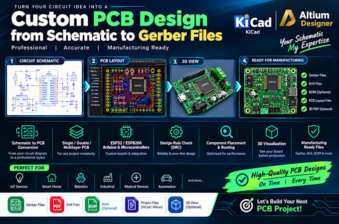
Need to convert your circuit schematic into a professional PCB layout?
I will transform your circuit diagram or schematic into a clean, organized, and manufacturing-ready PCB des-ign using KiCad or Altium Designer.
Whether you are developing an electronics prototype, an IoT device, an embedded system, or a custom microcontroller board, I can help you turn your idea into a practical PCB layout tailored to your project requirements.
WHAT I CAN DO FOR YOU
Ready to turn your schematic into a professional PCB?
Contact me with your project details, or select the package that best matches your requirements.