Browse categories
English
$
USD
Connect to your AI
Electronics Engineering Circuit Design Schematic Design
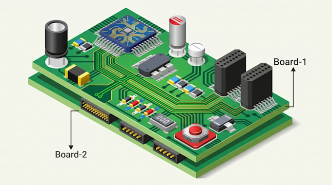
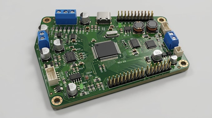
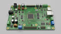
Preparing an electronic board for fabrication? I provide PCB layout, schematic capture and routing services to help organize your design for the manufacturing stage.
I can assist with component placement, resistor and capacitor networks, IC footprints, microcontrollers, connectors, diodes, transistors, power circuits, PCB traces, copper layers, ground planes, signal routing, SMD components, through-hole parts and board outlines.
My PCB preparation services include:
Schematic capture and circuit organization
PCB component placement
Single-layer and multilayer PCB layout
Signal and power trace routing
Copper and ground plane configuration
Design rule checks (DRC)
Gerber and NC drill files
Bill of materials (BOM), when required
Editable PCB project files
Final files can include:
Complete PCB layout
Routed circuit board design
Gerber fabrication files
NC drill files
Bill of materials (BOM), when required
Editable project files
Manufacturing drawings
Contact me with your existing schematic, PCB project or technical specifications, so i can go through the requirements and confirm board complexity and required manufacturing outputs before we begin.
Can you convert my schematic into a PCB layout?
Yes. Provide your schematic and component information, and I'll review it for PCB layout and routing.
Do you provide Gerber and NC drill files?
Yes, these can be included in the package according to the agreed project scope and fabrication requirements.
Do you check the PCB before delivering it?
I can perform applicable design rule checks and review the layout. Final fabrication approval should also follow your manufacturer's specific design rules.