i
isaacpams

ISAAC

@isaacpams

PCB Design and Layout Engineer

United Kingdom
French, Spanish, English
About me
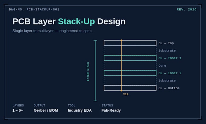
I’m a PCB Design and Layout Engineer specializing in schematic capture, PCB layout, multilayer board design, and manufacturing-ready electronics. I help startups, makers, and engineering teams turn circuit ideas into reliable PCBs. My services include component placement, trace routing, Gerber file generation, BOM preparation, and design optimization. Whether you need a simple prototype or a complex multilayer PCB, I focus on clean routing, manufacturability, and dependable performance with clear communication and attention to detail.... Read more

Skills

i
isaacpams
ISAAC
Offline • 
Average response time: 1 hour

See my services

Printed Circuit Boards (PCB)
I will wearable and medical device pcb, schematic, gerber and bom
Printed Circuit Boards (PCB)
I will design ble pcb for ecg, ppg and heart rate wearable devices

Work experience

PCBoost

Senior PCB & Hardware Design Engineer

PCBoost • Full-time

May 2019 - Present7 yrs 2 mos

Design and development of production-ready schematics and PCB layouts for AI edge hardware, wearable medical devices, IoT systems, and embedded electronics. Specialized in compact, low-power, and manufacturable PCB designs, with support for prototype and production deployment through trusted PCBA manufacturing partners. Delivered Gerber files, BOMs, assembly documentation, and optimized board layouts for single-layer, double-layer, and multilayer PCB projects. Worked closely with startups, inventors, and engineering teams to develop reliable hardware solutions ready for fabrication and assembly.