Browse categories
Explore
Fiverr Pro
English
$
USD
Smart PCB Design, Reliable Electronics, Ready for Production
Need a reliable RF PCB design, antenna design, or high speed PCB layout for your electronics project?
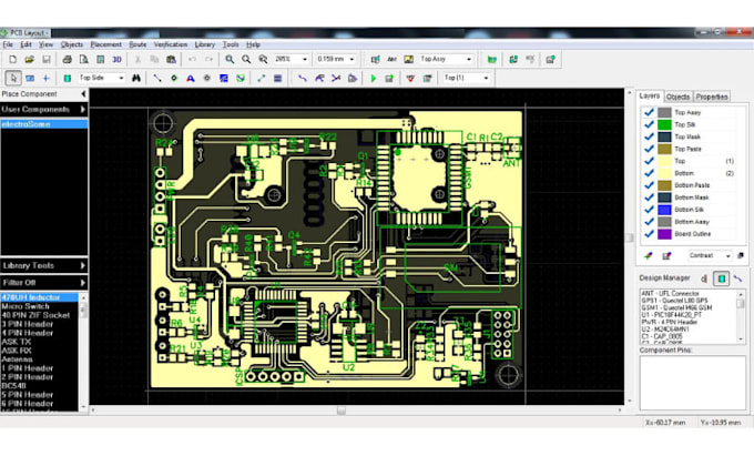
I can help transform your circuit concept or schematic into a clean, optimized, and manufacturing ready PCB design with careful attention to RF performance, signal integrity, impedance control, grounding, power distribution, and component placement.
Whether you're developing an IoT device, wireless product, RF module, embedded system, GNSS device, robotics platform, UAV electronics, or high speed digital board, I can create a PCB layout tailored to your project requirements.
What You Get
Contact me before placing your order so I can review your schematic, board requirements, layer count, dimensions, component list, antenna specifications, and other technical requirements.

Can you design an RF PCB from my schematic?
Yes. I can create the PCB layout from your schematic while considering RF routing, component placement, grounding, impedance requirements, and board constraints.
Can you design the antenna as well?
Yes. I can provide antenna design/layout support based on your required frequency, board dimensions, application, and available antenna area. If advanced electromagnetic simulation or laboratory validation is required, that should be discussed before ordering.
Do you handle high speed PCB routing?
Yes. I can handle high speed layouts involving differential pairs, controlled impedance, length matching, sensitive signal routing, power integrity considerations, and multilayer PCB structures.
What files do you need before starting?
Ideally, send your schematic, component/BOM information, board dimensions, layer requirements, target manufacturer capabilities, operating frequencies, interface specifications, and any existing PCB or mechanical files. If you don't have everything ready, contact me and I can tell you what is needed
Can you fix or optimize an existing PCB design?
Yes. I can review an existing PCB for routing problems, component placement, DFM issues, signal integrity concerns, grounding, and layout optimization.