Browse categories
Explore
Fiverr Pro
English
$
USD
Product Design Engineer, 3D CAD, Prototyping, Manufacturing and PCB Design
Level 2
Has met high performance criteria and has a proven track record for meeting client expectations.
Highly Responsive
Known for exceptionally quick replies
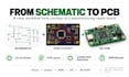
Professional PCB Design | Schematic to Manufacturing
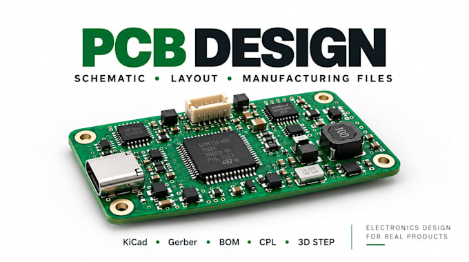
Need reliable PCB for a prototype or electronic product? I provide PCB design, schematic capture, circuit design and embedded hardware development with a focus on functionality, manufacturability and clean engineering.
PCB engineering is carried out by an Electrical Engineer with an MSc in Embedded Systems, with mechanical and enclosure integration support available when required.
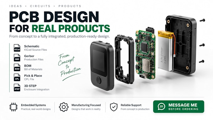
Services include:
Why work with me?
Please message me before ordering so I can review your requirements and recommend right package.

_vjcils.jpg)
What do you need from me to start the PCB design?
Please share your project requirements, functional description, preferred components, dimensions, power requirements, interfaces, reference files, and any existing schematic or PCB files. If you only have an idea, message me first and we can define the requirements together.
Can you design a PCB if I only have a product idea?
Yes. I can help convert your product requirements into a circuit schematic and PCB design. Component selection, interfaces, power architecture, board size, and manufacturing requirements can be discussed before starting.
What files will I receive?
Depending on the package, deliverables can include KiCad source files, schematic, Gerber files, drill files, BOM, Pick and Place/CPL files, fabrication files, PDF documentation, and a 3D PCB STEP model.
Do you design both the schematic and PCB layout?
Yes. I can provide complete schematic and PCB layout design, or work from an existing schematic if you only need PCB layout and routing.
Can you redesign or improve an existing PCB?
Yes. Existing PCB designs can be reviewed, modified, optimized, resized, rerouted, or updated for new components and manufacturing requirements. Please share the available source files before ordering.
Do you provide manufacturing-ready Gerber and BOM files?
Yes. Manufacturing-ready deliverables can include Gerber, drill, BOM, Pick and Place/CPL, and other fabrication files required by PCB manufacturers such as JLCPCB or PCBWay.
Which software do you use for PCB design?
KiCad is the primary PCB design platform. Source/project files can be provided where included in the selected package.
Can you help make the PCB fit inside my enclosure?
Yes. Mechanical and enclosure integration support is available. PCB dimensions, connector locations, mounting holes, clearances, and 3D STEP models can be coordinated with the enclosure design.
Is firmware or embedded programming included?
Firmware development is not automatically included in the PCB design packages. If your project requires firmware or embedded-system development, please contact me so the complete scope can be reviewed and quoted separately.
Should I contact you before placing an order?
Yes, please message me before ordering. PCB complexity can vary significantly depending on component count, layers, interfaces, power requirements, board dimensions, and design complexity. I will review your project and recommend the most suitable package or custom offer.