Browse categories
Explore
Fiverr Pro
English
$
USD
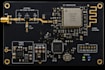
Looking for a professional RF PCB designer who understands high-frequency behavior and real-world RF layout challenges? I create reliable RF circuits and PCBs with proper antenna matching, impedance control, and clean routing for stable wireless performance.
I specialize in RF circuit design and PCB layout for Wi-Fi, Bluetooth, and other RF applications, ensuring controlled impedance traces, minimized noise, and optimized signal integrity. Whether youre building a prototype or preparing for production, I focus on designs that work in practice, not just on paper.
My RF follow industry-standard layout practices, including correct grounding, isolation, matching networks, and fabrication-ready outputs suitable for manufacturers.
What I offer:
Suitable for wireless modules, RF transceivers, IoT devices, and high-frequency PCB applications.
Please contact me before ordering to confirm RF frequency, board stack-up, and design requirements.

File format:
Gerber
•
STEP
•
SCH
•
•
Other
Software:
EasyEDA
•
LTspice
•
NI Multisim
•
Proteus
•
CST Studio Suite
Interface:
UART
•
SPI
•
I2C
•
Wi-Fi
•
BLE
•
BT
•
Ethernet
•
Other
What RF frequencies do you support?
I support common RF ranges used in Wi-Fi, Bluetooth, ISM band, and custom RF designs.
Do you handle antenna matching?
Yes, I design and optimize antenna matching networks based on your requirements.
Will the design be manufacturing-ready?
Yes, all designs include fabrication-ready Gerber files and proper RF layout practices.
