j
jadeclayton32

Jade Clayton

@jadeclayton32

PCB DESIGN ENGINEER

United Kingdom
English, German
About me
I am a professional PCB Design Engineer with strong experience in designing reliable, efficient, and production ready circuit boards for a wide range of electronic applications. My work combines technical precision, practical manufacturing knowledge, and performance optimization to deliver high quality hardware solutions. From concept development to final manufacturing files, I handle every stage of PCB design with accuracy and attention to detail. Each board is designed with proper component placement, optimized routing, controlled impedance... Read more

Skills

j
jadeclayton32
Jade Clayton
Offline • 
Average response time: 4 hours

See my services

Embedded Systems & IoT
I will configure sx1276 lorawan, lte cat m, azure iot, esp32 and gps tracker devices
Printed Circuit Boards (PCB)
I will design custom raspberry pi zero 2 wh extension board pcb with 2 20 smd header

Work experience

Tech_& Fix

PCB Design & Hardware Development Engineer

Tech & Fix • Self-employed

Mar 2020 - Present6 yrs 2 mos

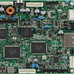
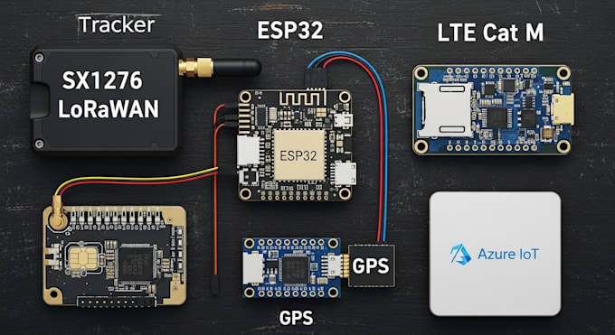
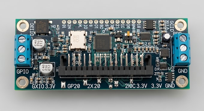
Designed and optimized custom printed circuit boards for embedded electronics and electronic device applications. Created schematics and PCB layouts for analog, digital, mixed signal, and power electronics systems using professional EDA tools. Managed component selection, BOM preparation, design rule validation, and manufacturing file generation. Performed hardware bring up, circuit troubleshooting, signal integrity verification, and prototype testing. Diagnosed board level faults, repaired PCB issues, and implemented design improvements for reliability and performance.