Browse categories
Explore
Fiverr Pro
English
$
USD
PCB Design Embedded Electronics Engineer
HELLO AND WELCOME
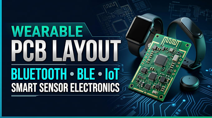
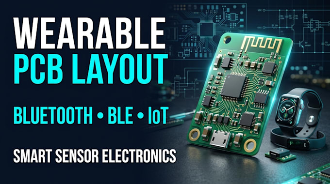
Developing a wearable device requires a compact, reliable PCB that supports Bluetooth connectivity and smart sensors without wasting valuable space. Poor component placement, unsuitable footprints, and inefficient power management can create design problems and costly revisions. I provide wearable PCB layout services for Bluetooth enabled devices, smart sensors, and compact electronics, helping turn your requirements into organized, manufacturing ready design files tailored to your project's needs.
WHAT I WILL OFFER
WHY CHOOSE ME
Send me your project requirements and let's create a compact, reliable PCB tailored to your device. Contact me today before ordering



What types of wearable PCBs do you design?
I work on compact PCB layouts for wearable devices, Bluetooth-enabled electronics, smart sensors, fitness trackers, smart bands, and IoT prototypes.
Can you integrate Bluetooth Low Energy (BLE) into my PCB?
Yes. I can help integrate BLE-capable modules or microcontrollers based on your connectivity requirements and device specifications.
Can you make the PCB fit my device's limited space?
Yes. Share your board dimensions, enclosure details, and component requirements so I can plan a compact layout and suitable component placement.
Can you integrate smart sensors into my PCB?
Yes. I can help integrate suitable motion, temperature, environmental, and other sensors according to your project's requirements.
Which files will I receive?
Depending on your selected package, deliverables can include schematics, PCB source files, Gerber files, BOM, PDF documentation, and pick-and-place files.
Do you provide firmware development?
Firmware support may be available depending on your selected package and project scope. Please specify your microcontroller and required functions before ordering.
Can you review or modify my existing PCB layout?
Yes. I can help update existing layouts, adjust component placement, improve routing, and review design issues based on the files you provide.
What do you need before starting the project?
Please provide your device requirements, PCB dimensions, schematic (if available), microcontroller, sensor list, battery specifications, connectivity needs, and preferred output formats.