Browse categories
Explore
Fiverr Pro
English
$
USD
Professional RF PCB Layout Engineer Wireless, Antenna and High Frequency Circuit
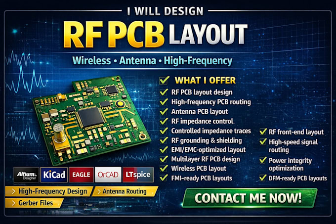
I'm a professional RF PCB layout engineer with 7+ years of experience in designing high-frequency, wireless, antenna, and RF circuit PCB layouts for reliable real world performance. I create production-ready RF PCB designs with controlled impedance, clean grounding, low noise, and strong EMI/EMC performance optimized for manufacturing and testing.
What I Offer:
What I Will Deliver:
Perfect For :
Software I Use:
Why Choose Me:
Contact me now

What types of RF PCBs can you design?
What types of RF PCBs can you design? A1: I design high-frequency, wireless, antenna, IoT, and communication RF PCBs with controlled impedance and EMI/EMC optimization
Will I get files ready for manufacturing?
Yes! I provide Gerber, drill, pick-and-place files, stack-up info, and all documentation needed for production
Can you handle multilayer RF PCB layouts?
Absolutely. I design multilayer RF PCBs optimized for signal integrity, impedance control, and low-noise performance
Do you support prototype-to-production designs?
Yes. I ensure your RF PCB works in prototypes and is ready for smooth transition to manufacturing
How do you ensure high-frequency signal quality?
I use advanced techniques like controlled impedance traces, proper grounding, shielding, and EMI/EMC aware routing for reliable performance
