Browse categories
Explore
Fiverr Pro
English
$
USD
HELLO BUYER!
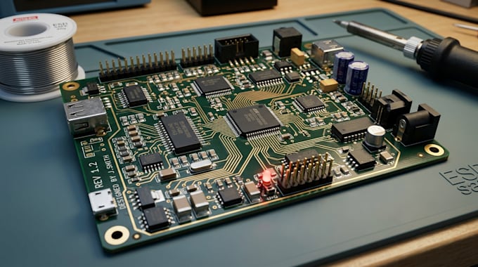
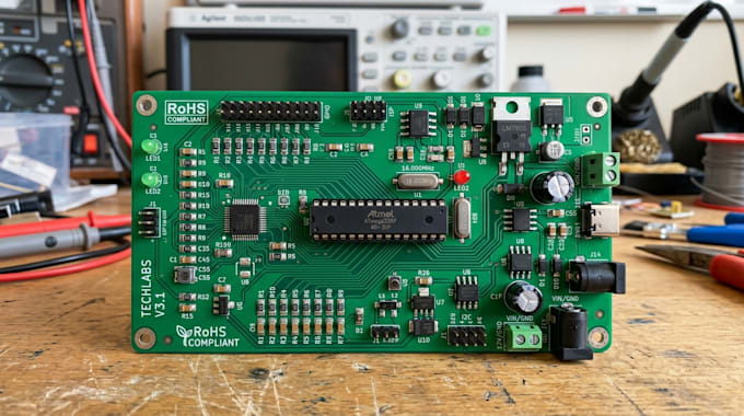
I am a professional Electronic Engineer specializing in PCB reverse engineering PCB cloning schematic recreation and manufacturing ready PCB design. Whether your original design files have been lost the board is discontinued or you only have images and a physical PCB I can accurately analyze reconstruct and recreate the design into professional engineering files. My goal is to help individuals startups repair technicians manufacturers and businesses recover valuable electronic designs and obtain complete documentation for future production .
WHAT I CAN DO:
WHY CHOOSE ME:
Please contact me before placing an order so I can review your PCB and recommend the most suitable package.
Specialization:
Circuit design
•
Schematics
•
Layout
•
Footprint
File format:
Gerber
•
SCH
•
Interface:
HDMI
•
I2S
•
UART
•
USB
•
SPI
•
I2C
•
SDIO
•
Wi-Fi
•
BLE
•
GSM/GPRS
What do you need to start the PCB reverse engineering project?
Please provide clear, high resolution photos of both sides of the PCB. If available include the PCB dimensions layer count BOM datasheets schematic or the physical board. The more information you provide the more accurate the recreated design will be.
Can you reverse engineer multilayer or obsolete PCBs?
Yes. I can reverse engineer single layer double layer and multilayer PCBs including obsolete or discontinued boards. For complex multilayer designs please contact me first so I can evaluate the board and provide an accurate quote and delivery time.
What files will I receive after the project is completed?
Depending on your selected package you can receive the schematic PCB layout Gerber files drill files Bill of Materials (BOM) Pick and Place files and editable source files in Altium Designer KiCad EasyEDA or Eagle.
Can you modify or improve the original PCB design?
Absolutely. In addition to recreating the original PCB I can update the layout replace obsolete components with modern equivalents optimize routing improve manufacturability and implement design changes based on your requirements.
Will the recreated PCB be ready for manufacturing?
Yes. Every completed design is prepared according to industry standards and delivered with manufacturing ready Gerber files and the required production documents allowing you to send them directly to your preferred PCB manufacturer.