Browse categories
Explore
Fiverr Pro
English
$
USD
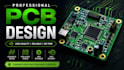
PCB Design and Schematic Expert, IoT and Circuit Solutions
Are you building the next smart IoT device but stuck on PCB design? I specialize in ESP32 based IoT PCBs that actually workno WiFi dropouts, no EMI headaches, no manufacturing surprises.
I design professional 4 layer PCBs with proper antenna matching, impedance controlled traces, and optimized stackups for ESP32, ESP32-S3, ESP32-C3, and ESP32-C6 modules.
WHAT YOU GET:
TOOLS I USE:
IDEAL FOR:
WHY 4-LAYER?
Better signal integrity, dedicated ground plane, cleaner power delivery, and proper antenna performance.
Let's turn your ESP32 idea into a production ready PCB. CONTACT ME NOW!

Do I need to provide a schematic?
No! I can work from your block diagram, rough sketch, or even just a description of what you want the device to do.
Which ESP32 modules do you support?
All of them—ESP32-WROOM, ESP32-WROVER, ESP32-S3-WROOM, ESP32-C3, ESP32-C6, ESP32-H2, and custom modules.
Can you design for JLCPCB/PCBWay assembly?
Yes, I optimize BOMs for their parts libraries and follow their design rules for seamless assembly.
What if I only need a 2-layer board?
I can do 2-layer for simple designs, but I recommend 4-layer for any RF or high-speed application. It costs only slightly more to manufacture but performs significantly better.
Can you help with FCC/CE certification?
I design with EMC best practices (proper grounding, filtering, shielding recommendations). For full certification support, check my Premium package or message me.
