Browse categories
Explore
Fiverr Pro
English
$
USD
IoT PCB and Embedded Systems Fusion 360 Product Design Expert
PROBLEM
Many ESP32 and wireless PCB designs fail due to poor RF layout, weak antenna performance, or EMI interference leading to short range, unstable connections, and costly redesigns.
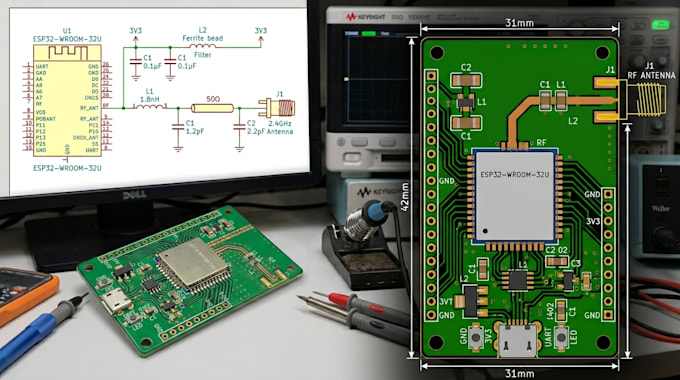
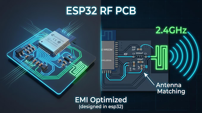
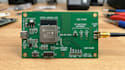
I will design a high-performance ESP32 2.4GHz RF PCB with proper antenna matching, clean layout techniques, and EMI-optimized routing to ensure reliable wireless communication.
SERVICES:
ESP32 PCB design (WiFi + BLE)
2.4GHz RF layout optimization
Antenna matching & placement
Impedance-aware routing
EMI/EMC reduction techniques (grounding, shielding)
Clean schematic & PCB layout
Gerber files ready for manufacturing
APPLICATIONS:
IoT devices, smart home systems, wearables, wireless sensors, automation products
WHY ME:
Focus on real RF performance, not just routing
Clean, manufacturable PCB layouts
Reduced signal loss and interference
Fast communication and revisions
️IMPORTANT:
Message me before placing an order to discuss your requirements and ensure the best results.
Lets build a reliable, production-ready wireless system.
Specialization:
Circuit design
•
Layout
•
Footprint
File format:
Gerber
•
STEP
•
VRML
•
SCH
•
3DS
Software:
EasyEDA
•
Fusion 360
•
KiCad
•
CircuitMaker
Interface:
HDMI
•
MIPI DSI/CSI
•
I2S
•
TDM
•
UART
•
USB
•
SPI
•
I2C
•
SDIO
•
Wi-Fi
•
BLE
•
BT