Browse categories
Explore
Fiverr Pro
English
$
USD
PCB DESIGN AND EMBEDDED SYSTEM EXPERT
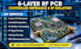
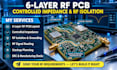
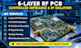
RF performance can be lost long before the first prototype is assembledpoor stackup choices, uncontrolled impedance, unwanted coupling, and weak grounding can turn a working schematic into a frustrating board. I help turn your RF requirements into a clean, manufacturable 6-layer PCB built around signal integrity and isolation.
What You'll Get
What Makes Me Stand Out
I focus on the problems that appear when RF signals share a crowded boardcoupling, noisy return paths, interference and routing compromisesrather than simply connecting traces.
Deliverables
Gerber files, drill files, PCB layout, fabrication-ready outputs and source files.
Have an RF board that needs a cleaner path from schematic to fabrication? Send your requirements and let's build it properly.
Can you create a complete 6-layer RF PCB from my schematic?
Yes. I can handle component placement, stackup planning, RF routing, controlled-impedance traces, grounding, isolation, and PCB checks based on your requirements.
Can you route controlled-impedance RF traces?
Yes. I can implement impedance-controlled routing according to your required impedance values, layer stackup, trace geometry, and PCB fabrication capabilities.
How do you handle RF isolation and interference?
I use appropriate layer planning, grounding, return paths, spacing, routing practices, and isolation techniques to reduce unwanted coupling between RF and other circuits.
What files do you need to get started?
Ideally, provide your schematic, PCB specifications, component/BOM files, required impedance values, preferred stackup or fabricator specifications, and any reference designs.
Will the PCB be ready for manufacturing?
Yes. Depending on the package, I can provide the PCB source files, Gerbers, drill files, and relevant fabrication outputs after DRC and manufacturing checks.


