Browse categories
Explore
Fiverr Pro
English
$
USD
Are you looking for a professional high-speed PCB specialist for a complex electronic hardware project?
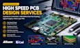
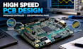
I will create high-speed, impedance-controlled PCB layouts with accurate USB differential pair routing, signal integrity considerations, and EMI-aware layout practices using Altium Designer or KiCad.
This service is suitable for embedded systems, SBC carrier boards, USB hubs, communication hardware, M.2 interfaces, 4G/5G modem systems, and other high-density electronic products.
My service includes:
High-speed PCB layout
Controlled impedance routing
USB differential pair routing
Multilayer PCB development
Schematic capture
Component placement and optimization
Ground plane and return path planning
EMI/EMC-conscious layout
Manufacturing-ready outputs
3D PCB visualization and STEP models
I work with Altium Designer and KiCad and can provide organized, production-ready project files based on your requirements.
Please contact me before ordering to discuss your PCB specifications, stackup, interfaces, mechanical constraints, and manufacturing requirements.
Let's turn your electronic concept into a reliable, professional, and manufacturing-ready PCB.
Specialization:
Circuit design
•
Schematics
•
Layout
File format:
Gerber
•
STEP
•
SCH
•
3DS
Software:
Allegro
•
Altium Designer
•
EasyEDA
•
KiCad
•
AutoCAD
•
Arduino
What PCB design software do you use?
I work primarily with Altium Designer and KiCad. I do not use EasyEDA for this service.
Can you design controlled impedance differential pairs?
Yes. I can design controlled impedance traces and differential pairs based on your PCB stackup and manufacturer's impedance requirements.
Can you design USB 2.0 and high-speed USB interfaces?
Yes. I can route USB interfaces while following differential pair routing, return path, length matching, spacing, and signal integrity considerations appropriate to the interface.
Do you design multilayer PCBs? and ground plane planning.
Yes. I can design multilayer PCBs for high-density and high-speed applications, including appropriate power
What files will I receive?
Depending on your selected package and project requirements, deliverables can include schematics, PCB source files, Gerber files, drill files, BOM, pick-and-place files, PDF documentation, and 3D STEP models.
Can you design PCBs for embedded systems and M.2/5G modules?
Yes. I can work on embedded hardware, SBC carrier boards, USB hubs, M.2 interfaces, communication hardware, and 4G/5G modem-related PCB projects.


