Browse categories
Explore
Fiverr Pro
English
$
USD
High Quality PCB Design for Every Project
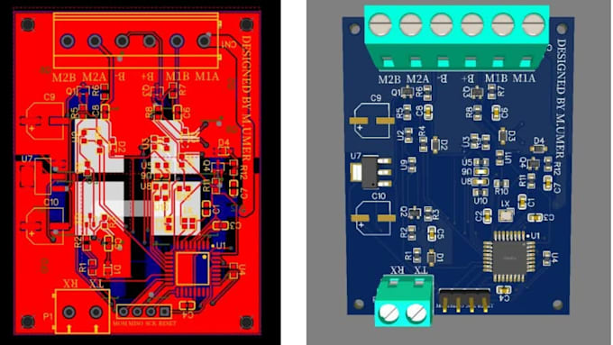
This service provides high-density, multi-layer PCB design and layout solutions for commercial electronics. I translate complex schematics into stable, production-ready circuit board files using Altium Designer and Cadence Allegro. The entire design cycle focuses on structural signal integrity, power distribution network optimization, and strict noise immunity.
DESIGN COMPLIANCE AND VALIDATION
Every layout undergoes rigorous Design for Manufacturing (DFM) and Design for Assembly (DFA) verification. By implementing precise impedance control, managed layer stackups, and targeted thermal dissipation paths, the final hardware is optimized to survive testing phases, prevent field failures, and achieve maximum manufacturing yield at the factory.
ADVANCED TECHNICAL DELIVERABLES:
Please provide your technical constraints and schematic files prior to ordering to ensure an accurate project scope assessment.