Browse categories
English
$
USD
Connect to your AI
Professional Multilayer PCB Reverse Engineering | 14+ Layers
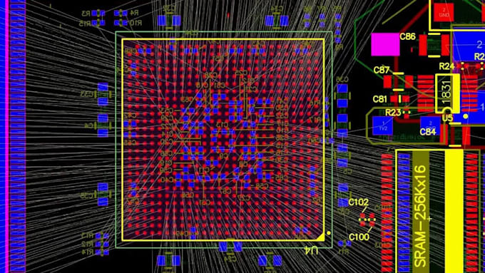
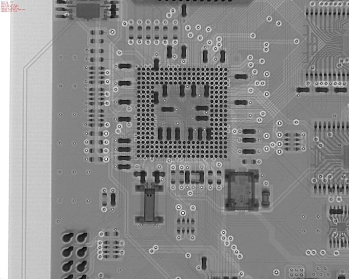
Do you need to reconstruct a complex multilayer PCB from an existing physical board, layer scans, X-ray images, or incomplete design files?
I am an Electronics Engineer with over 11 years of experience in PCB design, embedded hardware, and advanced multilayer PCB development.
My Services Include:
Supported Technologies:
DDR4, LPDDR4, USB 3.x, PCIe, HDMI, Ethernet, ARM-based systems, STM32, and complex embedded hardware.
Deliverables:

Can you reverse engineer a 14-layer or 20-layer PCB?
Yes, I can evaluate complex multilayer PCB reconstruction projects. Feasibility depends on the board structure, available layer images, via technology, and reference documentation. You can also deliver the PCB to me directly.
Can you reconstruct a PCB using photographs only
External photographs can support component placement and visible trace analysis, but they are generally insufficient to recover the internal routing of a 14+ layer PCB. Additional layer imaging or inspection data is usually required.
Do you support blind vias, buried vias, and BGA routing?
Yes. I can analyze HDI structures, BGA fanout, blind and buried vias, and multilayer routing when suitable reference data is available.
Which PCB design software do you use?
I work with Altium Designer and KiCad. Please specify your required editable file format before ordering.
Can you guarantee an identical replacement PCB?
An identical, fully functional replacement cannot be guaranteed from incomplete source data. Verification and physical prototype testing may be needed to confirm the reconstructed design.
Do you sign an NDA?
Yes. I can review and sign a reasonable non-disclosure agreement before receiving confidential project information.