Browse categories
Explore
Fiverr Pro
English
$
USD
ELECTRICAL ELECTRONICS, EMBEDDED SYSTEM AND PCB EXPERT
HELLO GREAT BUYER!!!
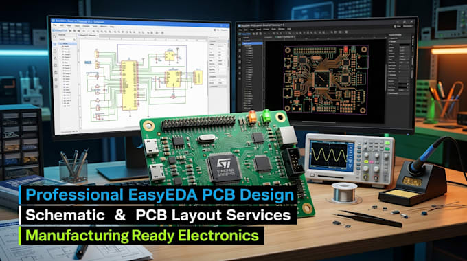
Professional schematic diagrams and PCB layouts are essential for reliable electronic device development, smooth manufacturing, and efficient circuit performance. A well optimized PCB design improves functionality, reduces errors, and ensures production ready electronic systems.
I will professionally create EasyEDA schematic diagrams and PCB layouts for electronic devices tailored to your project requirements.
What I Offer:
Why Choose Me:
Ready to turn your electronic idea into a professional PCB design? Send your requirements today and get high quality EasyEDA schematic and PCB layout services for your device!


File format:
Gerber
•
STEP
•
BRD
•
SCH
•
Software:
Altium Designer
•
Eagle CAD
•
EasyEDA
•
KiCad
•
AutoCAD
Interface:
HDMI
•
I2S
•
SPI
•
I2C
•
BT
•
LTE
What do you need to start my PCB project?
I need your circuit idea, component list, PCB dimensions, and reference files.
Do you provide Gerber files for manufacturing?
Yes, I provide manufacturing-ready Gerber files and PCB production documents.
Can you create multilayer PCB layouts?
Yes, I design single layer and multilayer PCB boards in EasyEDA.
Do you provide schematic diagrams?
Yes, schematic diagrams are included with PCB layout services.
Can you redesign or improve existing PCB boards?
Yes, I can optimize, modify, or redesign existing PCB layouts and schematics.
Which software do you use?
I use EasyEDA, Altium Designer, KiCad, and other professional PCB tools.