Browse categories
Explore
Fiverr Pro
English
$
USD

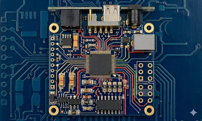
Professional PCB Design, PCB Layout and Electronics Engineering
Skills
See my services

Self Employed
Full-time • 2 yrs 10 mos
PCB Layout and Hardware Design Specialist
Sep 2020 - Sep 2021 • 1 yr
As a PCB Layout and Hardware Design Specialist, I was responsible for designing, modifying, and optimizing electronic circuits and printed circuit boards for various commercial and industrial applications. My role involved creating professional schematics, converting circuit concepts into manufacturable PCB layouts, troubleshooting design issues, and supporting prototype development for clients and engineering teams. I worked on numerous electronic projects including microcontroller-based systems, power supply circuits, motor control boards, wireless communication modules, LED controllers, sensor systems, and custom electronic products. My daily responsibilities included component selection, footprint creation, PCB routing, design validation, and preparation of production-ready files for manufacturing and assembly. A significant part of my work focused on optimizing PCB layouts for performance, reliability, and manufacturability. I performed signal routing, power distribution planning, grounding optimization, EMI reduction techniques, and thermal management considerations to ensure stable circuit operation. I also conducted design reviews and implemented engineering improvements to enhance product functionality and reduce manufacturing costs. In addition to PCB design, I supported prototype testing, debugging, and hardware validation processes. I worked closely with fabrication houses and assembly partners to ensure smooth production workflows and high-quality results. My experience in electronic hardware development allowed me to understand both engineering requirements and manufacturing constraints, helping clients achieve reliable and efficient product designs. Through strong technical knowledge, problem-solving abilities, and attention to engineering best practices, I consistently delivered professional PCB designs and hardware solutions that met client specifications and industry standards.
Senior PCB Design Engineer
Aug 2019 - Jun 2021 • 1 yr 10 mos
As a Senior PCB Design Engineer, I specialize in designing high-performance printed circuit boards for a wide range of electronic products and embedded systems. My responsibilities include schematic capture, PCB layout design, component selection, circuit analysis, signal integrity optimization, and manufacturing preparation. I work closely with startups, product developers, engineers, and manufacturing teams to transform concepts into reliable and production-ready electronic devices. Throughout my career, I have developed single-layer, double-layer, and multilayer PCB designs for consumer electronics, industrial automation systems, IoT devices, power management systems, communication modules, sensor interfaces, and embedded hardware solutions. My expertise includes creating detailed schematics, designing efficient PCB layouts, optimizing component placement, routing high-speed signals, and ensuring compliance with manufacturing standards. I have extensive experience using professional design tools such as Altium Designer, KiCad, EasyEDA, and Eagle PCB. I regularly generate manufacturing files including Gerber files, BOM documentation, pick-and-place files, assembly drawings, and fabrication documents. My workflow focuses on Design for Manufacturing (DFM), Design for Assembly (DFA), and design verification to minimize production issues and improve product reliability. I collaborate with clients throughout the entire product development cycle, from concept development and prototyping to testing and final production. By combining technical expertise with attention to detail, I deliver optimized PCB designs that meet performance requirements while maintaining cost-effective manufacturing processes. My goal is to provide high-quality electronic design solutions that help businesses accelerate product development and bring innovative products to market successfully.
