Browse categories
Explore
Fiverr Pro
English
$
USD
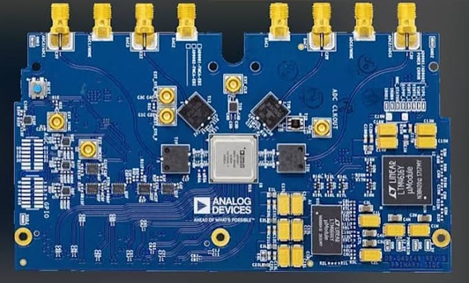
RF Network Interface Engineer Wireless Ethernet CAN High Speed PCB Solution
Need a custom PCB for wireless connectivity or industrial communication? Our engineering team develops schematics and board layouts for IoT products, sensors and embedded systems.
We work with module-based Wi-Fi, BLE, LoRa, cellular and GNSS designs, alongside Ethernet, CAN and RS-485 circuits. Before starting, we confirm your selected components, technical requirements and project scope.
Deliverables include:
Our design process considers RF routing, antenna clearance, grounding, power distribution and signal return paths.
Basic includes layout from your approved schematic. Standard adds circuit design. Premium covers two agreed communication circuits and a bring-up checklist.
Firmware, fabrication, assembly, lab testing and certification are excluded.
Send our team your specifications and board dimensions before ordering to confirm scope.


Specialization:
Circuit design
•
Schematics
•
Layout
•
Footprint
•
Gerber
File format:
Gerber
•
STEP
•
SCH
•
Circ
•
Pcbdoc
Software:
Altium Designer
•
Eagle CAD
•
EasyEDA
•
KiCad
•
Proteus
Is this service provided by a team?
Yes. Our engineering team manages your agreed schematic and PCB design scope. You receive coordinated communication and a consolidated set of project deliverables.
How is this different from your design-review gig?
This gig creates a new schematic or PCB layout within an agreed scope. Our review gig evaluates an existing design and provides findings and recommendations without creating or modifying the PCB.
Can your team design both wireless and wired interfaces?
Our listed scope includes module-based Wi-Fi, BLE, LoRa, cellular and GNSS circuits, alongside Ethernet, CAN and RS-485 interfaces. Send your component details first so we can confirm compatibility with our capabilities.
Which files will we receive?
Depending on your package, you receive PCB manufacturing exports, editable design files, a schematic, and a bill of materials. We agree on the CAD software, file formats, and manufacturing outputs before work begins.
Does the order include a working prototype or certification?
No. This gig delivers design files, not assembled hardware or certified performance. Fabrication, assembly, firmware, physical testing, and certification are separate activities. We can document the agreed design assumptions and test steps