I will design ble bluetooth pcb antenna for iot and wireless devices

United Kingdom

I speak English, German, Spanish

Expert PCB Cloning, Schematic Design Gerber File Creation

I am a PCB design and reverse engineering specialist helping businesses transform existing circuit boards into accurate digital engineering files. I specialize in PCB cloning, schematic recreation, P...
About this Gig

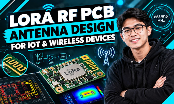
Need a compact and practical BLE antenna for your IoT or wireless device? I can help you create a PCB antenna layout that fits your project requirements


I provide BLE Bluetooth PCB antenna layout and RF integration services for IoT devices, wireless electronics, and prototypes. I focus on clean placement, proper RF routing, and an organized PCB layout.


What I offer:

  • BLE Bluetooth PCB antenna layout
  • Antenna placement and integration
  • RF trace routing
  • Matching network layout
  • Ground plane considerations
  • PCB layout recommendations
  • KiCad project files, where applicable
  • Layout review and design checks


Why choose me?

  • Clear and professional communication
  • Attention to PCB and RF layout details
  • Solutions tailored to your project
  • Organized and easy-to-use deliverables
  • Suitable for prototypes and IoT development

Whether you are building a BLE sensor, wearable device, smart home product, tracker, or another wireless project, send me your schematic, PCB dimensions, requirements, and reference files.


Message me before ordering so we can discuss your project and choose the right package.
Specialization:

Circuit design

•

Schematics

•

Layout

•

Simulations

File format:

Gerber

•

STEP

•

VRML

•

BRD

•

3DS

Software:

DipTrace

•

Eagle CAD

•

Fusion 360

•

KiCad

•

LabVIEW

•

AutoCAD

Interface:

HDMI

•

MIPI DSI/CSI

•

I2S

•

TDM

•

UART

•

USB

•

SPI

•

I2C

•

PCIe

•

Wi-Fi

•

BLE