Browse categories
Explore
Fiverr Pro
English
$
USD
ESP32 STM32 IoT BMS, EV Automotive PCB Design CAN Bus J1939 RF HighS
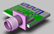
Professional RF PCB, High-Speed PCB, Antenna & Wireless Design
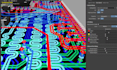
Need an expert PCB designer for your RF, wireless, or high-speed electronics project? I provide custom RF PCB design, multilayer PCB layout, antenna integration, and wireless hardware development tailored to your requirements.
MY SERVICES INCLUDE:
WHAT YOU WILL RECEIVE:
I focus on quality, precision, clean routing, and manufacturing-ready designs.
READY TO BRING YOUR ELECTRONICS PROJECT TO LIFE?

What information do you need to start the project?
Please provide your schematic, circuit diagram, PCB dimensions, layer requirements, component information, design specifications, and any existing reference files.
Can you design multilayer RF PCBs?
Yes. I can design 2-layer, 4-layer, and more complex multilayer RF/high-speed PCB layouts depending on the project requirements.
Do you provide Gerber and manufacturing files?
Yes. Depending on the selected package, I can provide Gerber, drill, BOM and other required manufacturing files.
Can you work with Altium or KiCad?
Yes. I can work with Altium Designer, KiCad, Eagle, EasyEDA and other PCB design platforms.


