Browse categories
Explore
Fiverr Pro
English
$
USD
PCB Designer
Looking for a reliable PCB designer who delivers clean, fabrication-ready boards? You're in the right place.
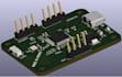
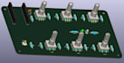
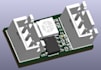
I'm Clinton, an Electrical & Electronics Engineer (BSc, DeKUT) specializing in PCB schematic capture and layout using KiCad 10. I design for embedded systems, IoT, and a wide range of electronics projects from simple 2-layer boards to complex 4-layer mixed-signal designs.
What I bring to your project:
Clean schematic design with proper documentation
Optimized PCB layout (correct trace widths, clearances, and power zoning)
Fabrication-ready files (Gerber, ODB++, STEP, BOM)
Experience with STM32, ESP32, and general embedded/IoT designs
My background includes hands-on industrial experience working with STM32-based telematics hardware (GPS/GSM systems), plus a range of personal and client projects including audio controllers, LED drivers, and IoT carrier boards.
Whether you have a finished schematic ready for layout, or need the full design built from scratch, I'll make sure your board is clean, efficient, and ready for manufacturing no back-and-forth, no guesswork.
Let's bring your idea to a working board. Message me before ordering
File format:
Gerber
•
STEP
•
SCH
•
•
ODB
Software:
Altium Designer
•
EasyEDA
•
KiCad
•
LTspice
•
Proteus
•
Arduino
Interface:
I2S
•
UART
•
USB
•
SPI
•
I2C
•
Wi-Fi
•
BLE
•
BT
•
GSM/GPRS


