Browse categories
Explore
Fiverr Pro
English
$
USD
Expert PCB Designer STM32 ESP32 Hardware Specialist RF Solutions
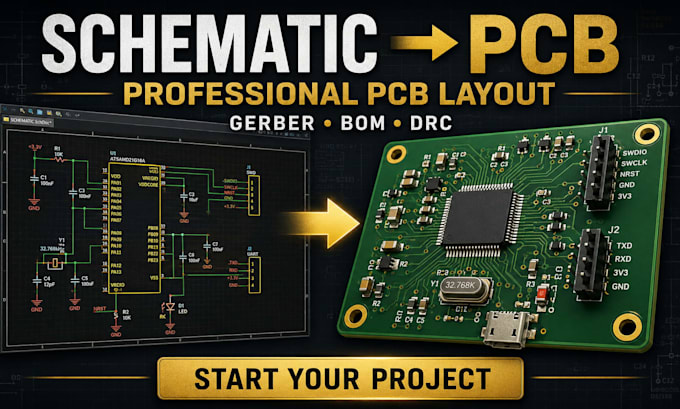
I will convert your existing schematic into a clean, organized and manufacturing-ready PCB layout with the required production files.
This service is ideal if you've already completed your circuit design and need an experienced PCB designer to turn it into a physical board layout.
WHAT I WILL DO
WHY THIS SERVICE?
A good schematic still needs careful translation into a practical physical PCB.
I focus on organized component placement, clean routing, appropriate spacing, and properly prepared manufacturing files.
IMPORTANT
This service is primarily for converting an existing electrical schematic into a PCB layout.
If you need circuit design, schematic creation, component selection, firmware, RF/antenna design, or advanced electronics engineering, please message me first so I can review the project and quote it correctly.
Send me your schematic and let's turn it into a professional PCB.



Do I need to have a schematic before ordering?
Yes. This gig is primarily for converting an existing schematic into a PCB layout. If you don't have a schematic, message me first so I can determine the appropriate service.
Can you convert a PDF schematic?
Yes, in many cases. However, the complexity and quality of the schematic should be reviewed before ordering.
Can you work from a hand-drawn schematic?
Potentially, depending on its clarity and complexity. Please send it for review before ordering.
Can you provide Gerber files?
Yes. Gerber files are included according to the selected package.
Can you provide the source files?
Yes, source/project files can be included according to the selected package.
Can you fix my schematic?
Schematic correction or circuit redesign is outside the basic conversion scope and may require a custom quote after technical review.
Can you convert my existing PCB to another software?
Yes, depending on the source files and target software. Please send the files first so the conversion requirements can be reviewed.