Browse categories
Explore
Fiverr Pro
English
$
USD
EMBEDDED SYSTEM AND FIRMWARE DEVELOPMENT
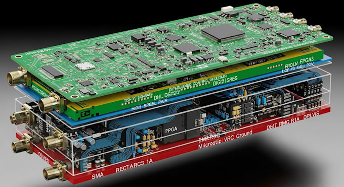
I specialize in controlled impedance routing, differential pair routing, PCB stack up design, ground plane optimization, and power integrity improvement. My layouts are carefully engineered to reduce EMI, minimize crosstalk, and maintain signal quality in complex multi-layer boards.
I have experience working with advanced processors and MCUs such as STM32H7, i.MX RT series, ESP32, and FPGA based platforms, integrating high speed interfaces like USB, Ethernet, LVDS, RF modules, and industrial communication systems.
Services I Offer
You will receive a professional, production ready PCB design optimized for both prototype development and mass production.
Please contact me before placing an order to discuss your PCB requirements, signal speeds, and hardware architecture.
What is considered a high-speed PCB design?
High-speed PCBs involve controlled impedance routing, differential pairs, and signal integrity techniques for fast digital or RF signals.
Can you design multi-layer high-speed PCBs?
Yes, I design multi-layer stack-ups optimized for signal integrity and power distribution.
Do you handle impedance-controlled routing?
Yes, I design traces with proper impedance control for high-frequency and differential signals.
Can you reduce EMI and crosstalk in PCB layouts?
Yes, I apply grounding, shielding, spacing, and routing strategies to minimize EMI and interference.
Do you design RF and mixed-signal PCBs?
Yes, I design RF routing, antenna sections, and mixed analog-digital boards.