Browse categories
Explore
Fiverr Pro
English
$
USD
Altium PCB Designer And Odoo ERP Expert for Scalable Systems
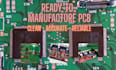
Get a professional Altium PCB design that is clean, accurate, and ready for manufacturing without costly errors or redesigns.
Many PCB designs fail due to poor routing, weak grounding, or a lack of proper signal and power integrity planning. This leads to unstable performance, failed prototypes, and delays in production. I help you avoid these issues by delivering well-structured schematic and PCB layouts built for real-world results.
I specialize in Altium PCB design for embedded and industrial electronics, ensuring your schematic and layout are fully aligned for electrical accuracy and manufacturability.
Services Included:
Using Altium EDA, your PCB will be designed with a clear structure, optimized performance, and production-ready outputs. Message me first to discuss your project and get it done right.

1. Can you design multilayer PCBs in Altium?
Yes, I design both simple and complex multilayer PCBs with proper routing and structure.
2. Will my PCB be ready for manufacturing?
Yes, you will receive Gerber files, BOM, and all required fabrication files.
3. Do you follow industry standards?
Yes, all designs follow best practices for signal integrity, grounding, and manufacturability.
4. Can you work from my existing schematic or idea?
Yes, I can design from scratch or improve your existing files.
5. What industries do you support?
Embedded systems, IoT, industrial electronics, and custom hardware projects.


