Browse categories
Explore
Fiverr Pro
English
$
USD
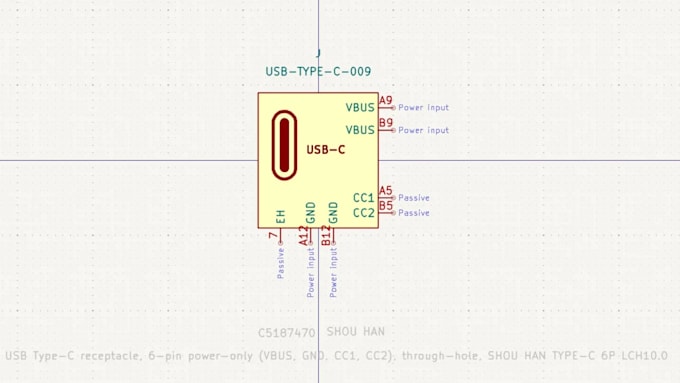
You get custom symbol and footprint directly from the manufacturer's actual datasheet real pad dimensions, correct drill sizes, and annular ring/clearance checked against your fab house's published capabilities (JLCPCB by default). Every pin name, number, and electrical type is set correctly so KiCad's ERC actually catches wiring mistakes instead of staying silent..
WHAT YOU GET;
Message me your datasheet or LCSC number and I'll confirm scope before you order.


Specialization:
Footprint
File format:
STEP
•
SCH
•
Pcbdoc
Software:
KiCad
Do you check against JLCPCB specifically, or other fabs?
JLCPCB by default; tell me your fab and I'll match their published drill/clearance specs.
What if the part already has an EasyEDA/LCSC listing?
I verify and clean it up rather than rebuilding — same price, faster turnaround.
Can you do connectors with non-standard pad layouts, not just ICs?
Yes — including through-hole parts with tight or irregular pin spacing.