Browse categories
English
$
USD
Connect to your AI
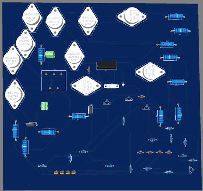
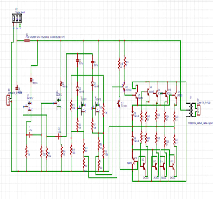
Are you looking for a reliable PCB designer for your electronics project?
I can help turn your circuit ideas into professional and well-organized printed circuit boards (PCBs). I focus on clean layouts, accurate component placement and proper routing to meet your project requirements.
My Services:
Why Choose Me?
I am committed to delivering quality work and helping bring your electronic ideas to life.
Please contact me before placing an order so we can discuss your requirements and project complexity.
Let's work together on your next electronics project!


Specialization:
Circuit design
•
Schematics
•
Layout
•
Footprint
File format:
Gerber
•
Software:
EasyEDA
•
KiCad
Interface:
UART
•
SPI
•
I2C
•
Wi-Fi