Browse categories
Explore
Fiverr Pro
English
$
USD
PCB Design, Circuit Design, Embedded Systems Engineer
Do you have an existing PCB but lost the original design files or schematic?
I will professionally reverse engineer your PCB and recreate the essential design files for documentation, redesign, repair, or manufacturing.
WHAT I CAN DO
WHY CHOOSE ME?
WHAT YOU WILL RECEIVE
Depending on your package, you can receive the recreated schematic, PCB layout, source project files, Gerber files, drill files, BOM and documentation.
Send your PCB photos, Gerbers, existing files, or available documentation before ordering so I can review the board complexity and confirm the correct package.

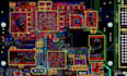
Can you reverse engineer a PCB from photos?
Yes, clear high-resolution photos of both sides can be used when sufficient information is visible.
Can you recreate the schematic and PCB layout?
Yes, depending on the board and information available.
Can you provide Gerber files?
Yes, applicable packages include manufacturing-oriented Gerber and drill outputs.
Do you work with Altium, KiCad and Eagle?
Yes
Can you work from existing Gerber files?
Yes. Existing Gerbers can help recreate the PCB layout and manufacturing information.
Can you handle multilayer boards?
Yes, but complexity and layer count should be reviewed before ordering.


