Browse categories
Explore
Fiverr Pro
English
$
USD
PCB Layout Specialist And Schematic to Manufacturing Ready Boards
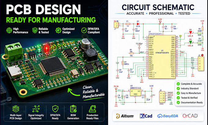
I design complete electronic circuits and PCB layouts that are ready for both prototyping and volume manufacturing. Whether you have an idea, a rough sketch, or an existing design to improve, I can turn it into clean schematics and fabrication files your PCB house can use directly.
WHAT I OFFER
DESIGN PRACTICES
TOOLS
KiCad, Altium Designer, EasyEDA (others on request).
Please contact me before ordering so we can review your specs, layer count, size constraints and deadlines, and choose the right package for your project.

What information do you need to start a PCB design?
To start the project, I typically need a schematic, component list (BOM), board dimensions, and any specific design requirements such as layer count or preferred components. If you have manufacturing requirements or reference designs, please include them as well.
What files will I receive after the project is completed?
You will receive manufacturing-ready files including Gerber files, drill files, PCB layout source files, and a bill of materials if required. These files can be sent directly to your PCB manufacturer.
Can you design a PCB from my idea or rough diagram?
Yes. If you have a concept, hand sketch, or functional description, I can help convert it into a proper circuit schematic and PCB design suitable for manufacturing.
Do you work with PCB manufacturers like PCBWay?
Yes. The designs I deliver are compatible with common manufacturers such as PCBWay and other PCB fabrication services. Gerber files are prepared according to standard manufacturing requirements.
Will my project remain confidential?
Yes. I respect client confidentiality and do not share project files or design information. If required, I can also work under a Non-Disclosure Agreement (NDA) before starting the project.
Should I contact you before placing an order?
Yes, contacting me first is recommended. This allows us to review the schematic, complexity, layer requirements, and timeline to ensure the correct package is selected.
Can you modify or improve an existing PCB design?
Yes. If you already have a PCB layout, I can review it, improve routing, optimize component placement, or prepare updated Gerber files for manufacturing.