I will design high speed multilayer pcb layout, schematic routing, kicad altium easyeda

Italy

I speak English, Italian, German, Spanish, French

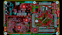
Professional PCB Design and Embedded Systems Engineer

I provide custom PCB layout and circuit schematic for Arduino, ESP32 using KiCad, Altium, EasyEDA. I handle high-speed multilayer PCB layout, routing, and signal integrity. Services include PCB design...
About this Gig

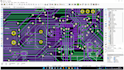
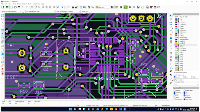
As an experienced Electronics and Electrical De sign Engineer, I specialize in delivering high-quality PCB de.sign, circuit d,esign, and PCB layout solutions tailored to your project needs. I create reliable and production-ready desi.gns for microcontrollers, IoT devices, Arduino, ESP32, and RF applications including multilayer PCB and impedance-controlled routing.


What I Offer:


  • Custom circuit desi,gn (analog, digital & mixed-signal)
  • Professional schematic design & PCB layout des.ign
  • RF PCB design, IoT PCB de.sign, and embedded PCB solutions
  • Gerber file generation & PCB prototyping support
  • BOM (Bill of Materials) with accurate components
  • 3D model/PCB visualization for better product understanding
  • DFM (Design for Manufacturing) optimization


Deliverables:


  • Schematic files
  • PCB layout files
  • Gerber & production-ready files
  • BOM file
  • PDF/PNG documentation of schematics and board
  • 3D PCB preview (on request)


I ensure clean, efficient, and manufacturable PCB board designs ready for real-world production.


Please message me before placing an order so we can discuss your idea and achieve the best possible result.

Specialization:

Circuit design

Schematics

Layout

Footprint

File format:

Gerber

STEP

VRML

PDF

ODB

Software:

Eagle CAD

EasyEDA

Fusion 360

KiCad

Arduino

CircuitMaker

Interface:

HDMI

MIPI DSI/CSI

I2S

UART

USB

SPI

SDIO

Wi-Fi

BLE

BT

GSM/GPRS

My Portfolio

Other Electronics Engineering Services I Offer