Browse categories
Explore
Fiverr Pro
English
$
USD
Electronic and Electrical Engineer
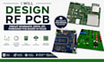
Many ESP32, RF PCB and IoT projects fail because of poor circuit schematic design, unstable PCB routing, signal interference, power issues or non manufacturable layouts. Without an experienced PCB designer, you risk wasted prototypes, device failures and expensive production errors that delay your project and reduce performance.
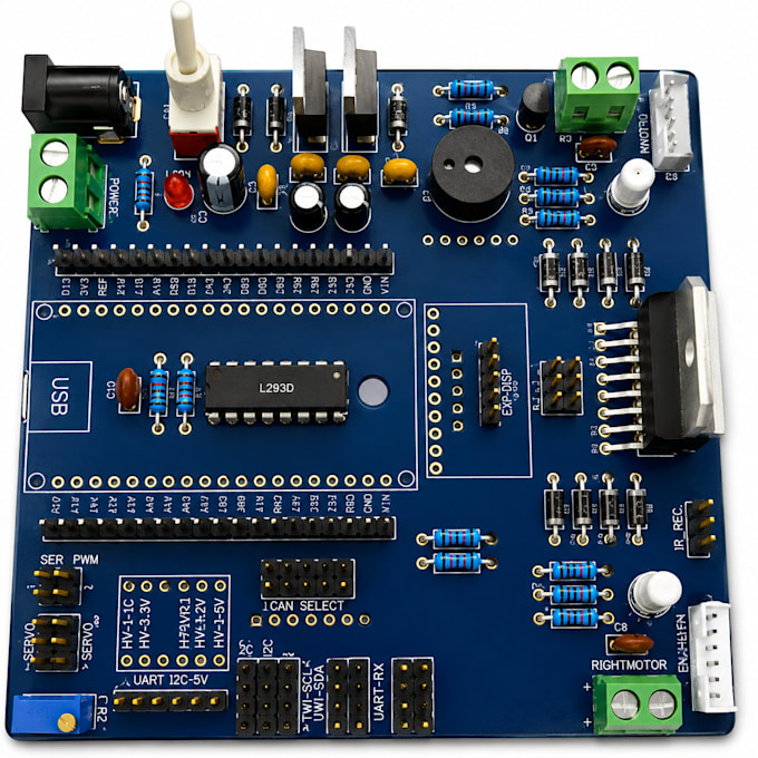
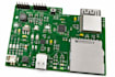
I will help you deslgn a professional RF PCB, circuit schematic, ESP32, IoT and embedded PCB board in KiCad with clean routing, reliable power distribution and production ready Gerber files. Whether you need an Arduino PCB, wireless module, embedded system or custom electronic circuit, you will get a design optimized for stability, functionality and manufacturing.
My service focuses on solving real hardware problems while improving signal integrity, PCB performance and production accuracy. You receive a clear schematic, organized PCB layout, DRC checked design, BOM and ready to manufacture files tailored to your project needs.
If you need a reliable KiCad PCB designer for your RF, ESP32 or embedded hardware project.
SEND ME A MESSAGE before ordering and lets build a high quality solution for your product.

Specialization:
Circuit design
•
Schematics
•
Layout
•
Footprint
•
Gerber
File format:
Gerber
•
STEP
•
BRD
•
SCH
•
Software:
Altium Designer
•
EasyEDA
•
KiCad
•
LTspice
•
Proteus
•
Arduino
What do you need to start my PCB project?
I need your project requirements, circuit idea, reference files, dimensions, preferred components and any existing schematic or block diagram.
Can you design ESP32, RF and IoT PCB boards in KiCad?
Yes, I design ESP32, RF PCB, IoT devices, embedded systems, Arduino PCB and custom electronic circuits using KiCad.
Will I receive manufacturing ready files?
Yes, you will receive Gerber files, PCB layout, circuit schematic, BOM and other production ready files for fabrication.
Can you help fix or improve an existing PCB design?
Yes, I can redesign, optimize and troubleshoot PCB layouts, routing, power issues and signal integrity problems.
Do you support multilayer and high speed PCB design?
Yes, I design 2 layer, 4 layer and multilayer high speed PCB layouts with proper grounding and routing techniques.