Browse categories
Explore
Fiverr Pro
English
$
USD
Design RF PCB Design, RF Layout, Antenna Design for Wireless and High Frequency
Looking for a accurate RF PCB Design Engineer for your wireless communication project? You are in the right GIG.
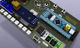
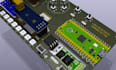
I focused on RF PCB Design, RF Layout, Antenna Design, Wireless PCB Design, and High Frequency PCB Development for IoT devices, RF modules, embedded systems, wireless communication products, and industrial electronic.
Whether you need a WiFi PCB, Bluetooth PCB, LoRa PCB, Zigbee PCB, GPS PCB, GSM PCB, LTE PCB, or custom RF hardware, I can design a high performance and manufacturing ready solution tailored to your requirements. Every deslgn is optimized for signal integrity, impedance matching, RF routing, EMI/EMC performance, antenna integration, and reliable wireless communication.
My service include RF PCB Deslgn, RF Layout, Antenna Deslgn, High Frequency PCB Deslgn, RF Circuit Deslgn, Wireless PCB Deslgn, PCB Antenna Deslgn, Impedance Matching, RF Routing, Signal Integrity Optimization, and Manufacturing File Generation.
RF PCB Deslgn, RF Layout, Antenna Deslgn, Wireless PCB, High Frequency PCB, RF Circuit Deslgn, LoRa PCB, WiFi PCB, Bluetooth PCB, GSM PCB, LTE PCB, GPS PCB, PCB Antenna Deslgn, RF Engineering, Signal Integrity, Impedance Matching.
CONTANT NOW
Specialization:
Circuit design
•
Layout
•
Analysis
•
Gerber
File format:
STEP
•
SCH
•
3DS
•
Software:
Altium Designer
•
Cadence OrCAD
•
DipTrace
•
Eagle CAD
•
KiCad
What information do you need to start my RF PCB project?
I need your project requirements, operating frequency, circuit specifications, block diagram, and any reference documents.
Can you design RF PCBs for WiFi, Bluetooth, LoRa, GSM, GPS, and LTE applications?
Yes, I design RF PCBs for WiFi, Bluetooth, LoRa, Zigbee, GSM, GPS, LTE, and other wireless communication systems.
Do you provide antenna design and integration?
Yes, I can design PCB antennas, chip antennas, and integrate external antennas for optimal RF performance.
Will I receive manufacturing ready files?
Yes, I provide Gerber files, BOM, Pick and Place files, assembly drawings, and all files required for PCB manufacturing.
Can you optimize my existing RF PCB design?
Yes, I can review and improve RF layouts, antenna placement, impedance matching, and signal integrity.
Which PCB design software do you use?
I work with KiCad, Altium Designer, EasyEDA, Eagle, and other professional PCB design tools.
Why should I contact you before placing an order?
Contacting me first allows us to discuss your requirements, project complexity, timeline, and ensure the best solution for your RF PCB design.


