Browse categories
English
$
USD
Connect to your AI
PCB Designer and Firmware Development
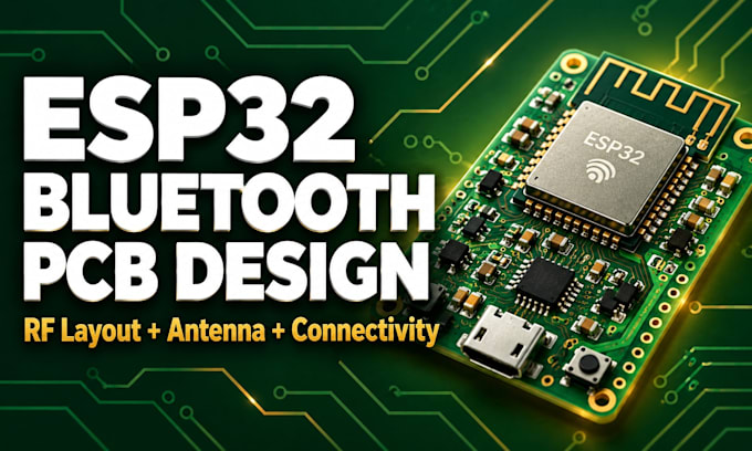
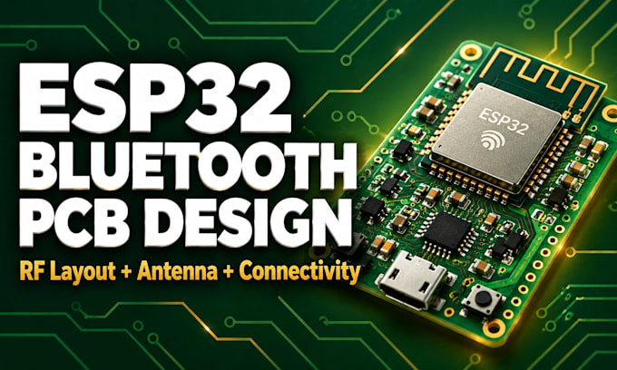
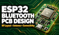
Need an ESP32 Bluetooth PCB that connects reliably? I design custom ESP32 PCBs with professional RF layout, antenna design and connectivity solutions for IoT, BLE and Wi-Fi products.
I turn your idea, sketch or schematic into a clean, manufacturing ready board for ESP32, ESP32-S3, ESP32-C3 and ESP32-WROOM modules.
WHAT I DESIGN
WHAT YOU GET
WORKS WITH: KiCad, Altium and Eagle
WHY CHOOSE ME
Send me your project details and let's get your ESP32 board working.
Which ESP32 modules do you work with?
ESP32 chips and modules, including ESP32-S3, ESP32-C3 and ESP32-WROOM. Send me your project and I'll confirm it's a good fit.
Will the files work with JLCPCB or PCBWay?
Yes. I deliver Gerber and drill files checked against standard manufacturer rules, so they are ready to send to any PCB fab.
Can you improve my existing ESP32 board?
Yes. Send your current files and describe what isn't working, and I'll let you know how I can help.